


Class 12 Physics Chapter 14 - Semiconductor Notes PDF - Free Download
Related Chapters


Section-A (1 Mark Questions)
1. Name two factors on which electrical conductivity of a pure semiconductor at a given temperature depends.
Ans. (i) The width of the forbidden band (ii) Intrinsic charge carrier concentration.
2. Why does the conductivity of a semiconductor increase with rise of temperature?
Ans. When a semiconductor is heated, more electrons jump across the forbidden gap from valence band to conduction band where these are free to conduct electricity. Hence the conductivity increases with the increase in temperature.
3. Why does a semiconductor get damaged when a heavy current flow through it?
Ans. When a heavy current flow, the semi-conductor gets heated up. Many covalent bonds break liberating a large number of free electrons. The semi-conductor loses its property of controlled conduction. It becomes an ordinary conductor.
4. The conductivity of an intrinsic semi-conductor is very low. Why?
Ans. An intrinsic semiconductor has a very small concentration of free electrons and holes (≈1016m−3) so it has low conductivity.
5. The forbidden energy band of silicon is 1.1eV. What does it mean?
Ans. This means that if an energy of 1.1 eV is given to an electron in the valence band, it will jump to the conduction band.
6. What is a hole? Which type of doping creates a hole?
Ans. A hole is vacant state in the covalent bond of a semiconductor from which an electron has been removed. When semiconductor is doped with trivalent impurity atoms of B, Al or In holes are created.
7. Why is germanium preferred over silicon for making semiconductor devices?
Ans. This is because the energy gap for Ge (Eg = 0.7eV) is smaller than the energy gap for Si (Eg = 1.1eV).
8. Why is the conductivity of n-type semiconductor greater than that of the p-type semiconductor even when both of these have same level of doping?
Ans. This is because under a given electric field, free electrons have higher mobility than holes.
9. Why does a potential barrier set up across a junction diode?
Ans. The accumulation of negative charges in the p-region and positive charges in the n-region sets up a potential difference across the junction. This is called potential barrier which opposes the diffusion of electrons and holes across the junction.
10. Can we measure the potential difference of a p-n junction by connecting a sensitive voltmeter across its terminals?
Ans. No, there are no free charge carriers in the depletion region. So, it offers infinite resistance in the absence of any forward biasing.
Semiconductor Class 12 Notes - Section-B (2 Marks Questions)
11. Why is a NOT gate known as an inverter?
Ans. A NOT gate always inverts the input. If input is low (0), the output is high (1) and vice versa. Hence a NOT gate is known as an inverter.
12. C, Si and Ge have same lattice structure. Why is C a insulator while Si and Ge are intrinsic semiconductors?
Ans. The 4 bonding electrons of C, Si and Ge lie, respectively, in the second, third and fourth orbit. Hence, the energy required to take out an electron from these atoms will be least for Ge, followed by Si and highest for C. Hence, the number of free electrons for conduction in Ge and Si and quite significant but negligibly small for C.
13. Why are the NAND and NOR gates known as digital building blocks or universal gates?
Ans. The repeated use of NAND or NOR gates alone can give all other gates like OR, AND and NOT gates. In digital circuits the NAND or NOR gates serve as building blocks and hence they are named so.
14. Draw a circuit diagram for p-n junction diode in forward bias. Sketch the voltage-current graph for the same.
Ans.


15. What is doping in semiconductor? Why is it done?
Ans. Doping is the process of addition of small amounts of certain specific impurity atoms valency different from that of host atoms to a pure semiconductor. Doping is done to increase the number of mobile electrons/holes and hence to increase the conductivity of a semiconductor.
16. Draw a circuit diagram for the reverse biased p-n junction diode. Sketch the voltage current graph for the same.
Ans.


17. In the following diagrams, diagrams, which of the diodes are forward biased and which are reverse biased.


(i)
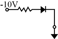
(ii)

(iii)
Ans.
(i) Forward biased, because p-side is at higher potential (+ 7 V) than n-side (+5V)
(ii) Reverse biased, because p-side is at lower potential (0V) than n-side (+2V)
(iii) Reverse biased, because p-side is at lower potential (-10V) than n-side (0V).
(iv) Forward biased because p-side is at higher potential (-5V) than n-side (-12V)
18. Give the symbol, and the truth table of each of the two logic gates, obtained by using the two gate combinations, shown in figure.

(a)

(b)
Ans. (a) The gate combination of figure (a) represents a NAND gate

Truth table of NAND Gate
(b) The gate combination of figure. (b) represents a NOR gate

Truth table of NOR gate
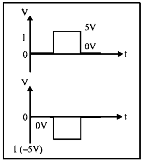
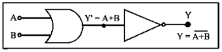
19. Draw the output waveform at X, using the given inputs A and B for the logic circuit shown below. Also, identify the logic operation performed by this circuit.

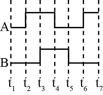
Ans. $Y=\overline{A+B}$ $X=\overline{Y}=A+B$ .
Thus, the given circuit performs OR operation. The output waveform obtained at X is of the type shown below.

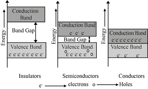
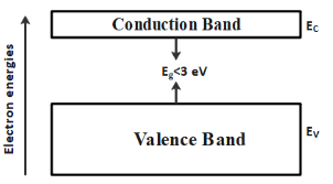
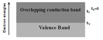
20. Distinguish between a conductor, a semiconductor and an insulator on the basis of energy band diagrams.
Ans.
PDF Summary - Class 12 Physics Semiconductor Devices & Communication System Notes (Chapter 14)
1. Energy Bands in Solids:
In the case of solids, there are single energy levels where the atoms are arranged in a systematic space lattice and therefore the atom is highly influenced by the neighboring atoms for a single isolated atom. The closeness of atoms will be resulting in the intermixing of electrons of the neighboring atoms of course, for the valence electrons, not strongly bounded by the nucleus, in the outermost shells. Because of the intermixing the number of permissible energy levels will be increased or there will be significant variations in the energy levels. Therefore, instead of single energy levels related with the single atom in the case of a solid, there will be bands of energy levels.
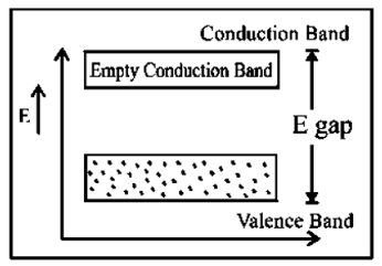
1.1. Conduction Band, Valence Band & Forbidden Energy Gap:
The band created by a series of energy levels including the valence electrons can be defined as valence band. The valence band can be explained as a band which is inhabited by the valence electrons or a band which is having highest inhabited band energy.
The conduction band can be explained as the least unfilled energy band. The forbidden energy gap can be defined as the separation between conduction band and valence band. There will be no permitted energy state in this gap and therefore electron can’t occupy in the forbidden energy gap.
1.2. Conductors, Semiconductors and Insulators:
Conductors are the materials which can conduct the charge carriers easily. Insulators are the materials in which the free flow of charge carriers is not possible. And semiconductors are the materials which have conductivity in between insulators and conductors.
According to the forbidden band, the insulators, semiconductors and conductors can be explained as mentioned below:
1.2.1. Insulators:
The forbidden energy band will be very wide in case of insulators. Because of this information electrons will not be jumped from valence band to conduction band. The valence electrons will be bond very tightly to their parent atoms in insulators. Increase in temperature will be enabling some electrons to move to the conduction band.
1.2.2. Semiconductors:
The forbidden band will be very small in semiconductors. Silicon and Germanium can be taken as the examples of semiconductors.
A semiconductor material will be the one having electrical characteristics lying between insulators and good conductors. If a little amount of energy has been supplied, the electrons can jump from valence band to conduction band easily. As an example, if the temperature will be enhanced, then the forbidden band will be reduced such that some electrons are liberated into the conduction band.
1.2.3. Conductors:
There will be no forbidden band and the valence band and conduction band overlap each other, in case of the conductors. Here a lot of free electrons will be available for the conduction of electricity. A small potential difference across the conductor will be causing the free electrons for including the electric current. The very relevant point in conductors is that because of the absence of forbidden band, there will be no structure for establishing holes. The summation of current in conductors will be simply a flow of electrons.
2. Semiconductors:
Hence, semiconductor can be defined as a substance which is having resistivity in between conductors and insulators.
Semiconductors will be having the properties mentioned below.
(i) They will be having less resistivity than insulators and more than conductors.
(ii) The resistance of semiconductor will be reduced with the increase in temperature and vice versa.
(iii) If suitable metallic impurity such as arsenic, gallium etc. will be added to a semiconductors, its current conducting characteristics varies appreciably.
2.1. Impact of temperature of Semiconductors:
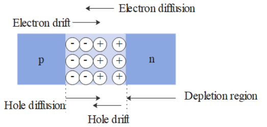
The semiconductor crystal will be acting like a proper insulator since the covalent bonds are pretty much strong and no free electrons are available. At room temperature, some of the covalent bonds will be broken due to the thermal energy given to the crystal. Due to the breakage of the bonds, some electrons will be free which were inhabited in the production of these bonds.
The non-appearance of the electron in the covalent bond can be represented by a small circle. Therefore Hole can be shown as an empty place or vacancy left behind in the crystal structure. Since an electron is having unit negative charge, the hole will be similarly having a unit positive charge.
2.2. Mechanism of conduction of Electrons and Holes:
If the electrons are released on the breakage of the covalent bonds, they will be moving randomly through the lattice of crystal.
If an electric field has been applied, these free electrons will be having a uniform drift which is opposite to the direction of field applied. This can be referred to as the electric current. If a covalent bond is broken, a hole has been produced. One hole is produced when one electron sets free. This thermal energy will be producing electron-hole pairs-there will be as many holes as free electrons. These holes can go through the crystal lattice in a random fashion such as free electrons. The holes drift in the direction of the applied field, if an external electric field is applied. Hence, this can be referred to as electric current.
There will be a strong tendency of semiconductor crystals for producing covalent bonds. Hence, a hole will be attracting an electron from the neighboring atom. Now a valence electron from nearby covalent bond will be coming for occupying in the hole at \[\text{A}\]. This will cause in a production of hole at \[B\]. The hole will be therefore successfully shifted from \[A\] to \[B\]. This hole will be moving from \[\text{B}\] to \[C\] from \[C\] to \[D\] and so on.
This movement of the hole in the non-appearance of an applied field will be random. But the hole gets drifted along the applied field, if an electric field has been applied.
2.3. Generation and Recombination of Carrier:
The electrons and holes will be produced in pairs. The free electrons and holes will move within the crystal lattice in an irregular manner. There is always a chance that an electron which is free will be meeting with a hole, in such a random motion. If a free electron encounter a hole, they will recombine for re-establishing the covalent bond. Both the free electron and hole will be destroyed in the process of recombination and cause in the emission of energy as heat. The energy produced thereby, may in turn will get re-absorbed by another electron for breaking its covalent bond. In this manner a new electron-hole pair will be generated.
Hence, the method of splitting of covalent bonds and recombination of electrons and holes will be taking place simultaneously. If the temperature will be increased, the rate of generation of electrons and holes will be enhanced. This is turn increases, the densities of electrons and hole will get increased. Because of this the conductivity of semiconductor will be increased or resistivity decreased. This will be the reason that semiconductors is having negative temperature coefficient of resistance.
2.4. Pure or Intrinsic Semiconductor and Impure or Extrinsic Semiconductors:
Intrinsic semiconductor can be defined as a semiconductor in which electrons and holes are solely produced by thermal excitation or a semiconductor in an extremely pure form is referred as a pure or intrinsic semiconductor. The number of free electrons will be always equivalent to the number of holes in intrinsic semiconductor.
2.4.1. Extrinsic Semiconductors:
The electrical conductivity of intrinsic semiconductor will be enhanced by the addition of some impurity in the method of crystallization. The added impurity will be very small of the order of one atom per million atoms of the pure semiconductor. This kind of semiconductor can be referred as impurity or extrinsic semiconductor. The method of infusing impurity to a semiconductor can be defined as doping.
The doping material will be either pentavalent atoms such as bismuth, antimony, arsenic, phosphorus which are having five valence electrons or trivalent atoms such as gallium, indium, aluminium, boron which are having three valence electrons. The pentavalent doping atom can be referred as donor atom since it is donating one electron to the conduction band of pure semiconductor.
The doping materials can be referred as impurities as they change the structure of semiconductor crystals which are pure.
2.4.2. N–Type Extrinsic Semiconductor:
If a little amount of pentavalent impurity has been added to a pure semiconductor crystal while the crystal growth, the produced crystal can be referred as N-type extrinsic semiconductor.
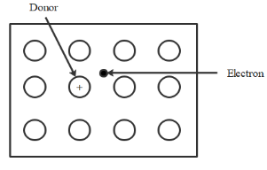
The following points should be remembered in case of N-type semiconductor
(i) The electrons will be the majority carriers while positive holes are minority carriers, in N-type semiconductor.
(ii) Even though N-type semiconductor is having excess of electrons but it will be electrically neutral. This will be because of the fact that electrons are produced by the addition of neutral pentavalent impurity atoms to the semiconductor. That is, there will be no addition of either positive or negative charges.
2.4.3. P–Type Extrinsic Semiconductor:
If a little amount of trivalent impurity has been added to a pure crystal while the crystal growth, the produced crystal can be referred as P-type extrinsic semiconductor.
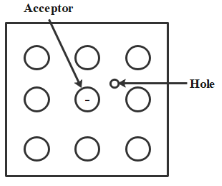
The following points should be remembered in case of P-type semiconductor:
(i) The majority carriers are positive holes but minority carriers are the electrons in P-type semiconductor materials.
(ii) The P–type semiconductor will be remaining electrically neutral as the number of mobile holes under all conditions remains equivalent to the number of acceptors.
2.5. P–N Junction Diode:
If a P-type material has joined to N-type intimately, a P-N junction will be created. Joining the two pieces a P-N junction will not be formed due to the surface films and other irregularities creating major discontinuity in the crystal structure. Hence, a P-N junction will be created from a piece of semiconductor (say, germanium) by diffusing P-type material to one half side and N-type material to the other half side. If a P-type crystal has kept in contact with N-type crystal so as to produce one piece, the assembly required will be defined as P-N junction diode.
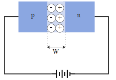
2.5.1. Forward Bias:
The junction diode can be defined as forward biased, if external d.c. source has been connected to the diode with p–section connected to positive pole and n–section connected to negative pole.
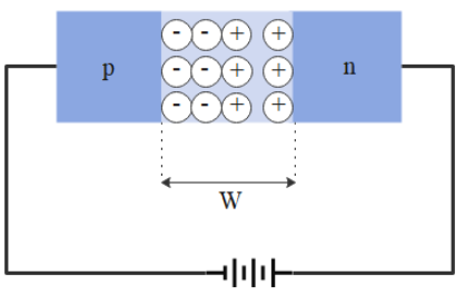
2.5.2. Reverse Bias:
The junction diode can be defined as reverse biased, if an external d.c. battery has been connected to junction diode with P–section connected to negative pole and n–section connected to positive pole.
Note:
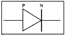
P–N JUNCTION can be defined as a device which will be offering low resistance when forward biased and act as an insulator if reverse biased.
Symbol:
2.6. Junction Diode as Rectifier:
An electronic device which will be transforming a.c. power into d.c. power can be defined as a rectifier.
2.6.1. Principle:
If forward biased, Junction diode will be offering a low resistive path and high resistance if reverse biased.
2.6.2. Arrangement:
The a.c. supply will be given across the primary coil (\[\text{P}\]) of step down transformer. The secondary coil ‘\[\text{S}\]’ of transformer will be in connection to the junction diode and load resistance \[{{\text{R}}_{\text{L}}}\]. The output d.c. voltage will be received across \[{{\text{R}}_{\text{L}}}\].
2.6.3. Theory:
Assume that when the first half of a.c. input cycle occurs, the junction diode will be forward biased. The conventional current will be flowing in the direction of arrow heats.
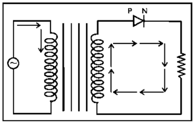
The upper end of \[{{R}_{L}}\] will be at positive potential with respect to the lower end. The magnitude of output across \[{{R}_{L}}\] while first half at any moment will be proportional to magnitude of current through\[{{R}_{L}}\], which in turn will be proportional to magnitude of the forward bias and which will be dependent upon the value of a.c. input at that time ultimately.
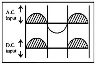
Hence, output across \[{{R}_{L}}\] will be changing with respect to a.c. input. During the second half, the junction diode will be getting reverse biased and therefore no–output will be there. Hence, a discontinuous supply will be received.
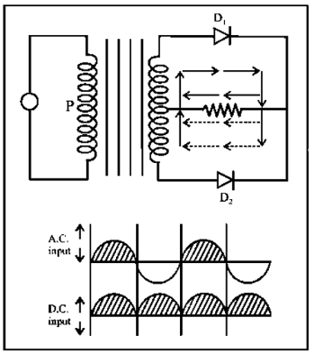
2.7. Full Wave Rectifier:
A rectifier which will be rectifying both halves of a.c. input can be referred as full wave rectifier.
2.7.1. Principle:
Junction Diode will be giving low resistive path if forward biased and high resistive path if reverse biased.
2.7.2. Arrangement:
The a.c. supply has been supplied across the primary coil (\[P\]) of step down transformer. The two ends of S–coil (secondary) of transformer will be connected to P-section of junction diodes \[{{D}_{1}}\] and \[{{D}_{2}}\]. A load resistance \[{{R}_{L}}\] will be connected across the n–sections of two diodes and central tapping of secondary coil. The d.c. output will be received across secondary.
2.7.3. Theory:
Assume that while first half of input cycle upper end of s-coil will be at \[+ve\] potential. The junction diode \[{{D}_{1}}\] will be getting forward biased, while \[{{D}_{2}}\] will be getting reverse biased. The conventional current because of \[{{D}_{1}}\] will flow along path of full arrows.
If second half of input cycle comes, the conditions will be in opposite manner. Now the junction diode \[{{D}_{2}}\] will be conducting and the conventional current will be flowing along path of the dotted arrows. The output during both the half cycles will be of similar nature as the current during both the half cycles flows from right to left through load resistance \[{{R}_{L}}\].
The right end of \[{{R}_{L}}\] will be at \[+ve\] potential in accordance with left end. Hence, the output will be continuous in full wave rectifier.
Special usages of P-N junction Diode:
(a) Zener Diode:
The zener diodes can be defined as a heavily doped P-N junction diode where the operation of the device can occur only in the reverse biased condition. Here as both p and n sides are heavily dope, the depletion region developed will be very thin. In this diodes, when the applied reverse bias voltage reaches the breakdown voltage of the zener diode, we can see a huge variation in the current. At this time, the reverse voltage will be almost a constant even though there is significant change in the current occurs. Hence this kind of diodes can be used a voltage regulators.
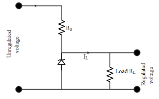
The above shown image is showing the Zener diode as a DC voltage regulator.
Here we have to choose the Zener diode in accordance to the needed output voltage and the series resistance Rs accordingly.
2.8. Transistor:
This will be a three section semiconductor, where three sections are combined so that the two at extreme ends will be having similar kind of majority carriers. At the same time, the section that is separating them will be having the majority carriers in opposite nature. The three sections of transistor can be defined as emitter (\[E\]), Base (\[B\]) and collector \[(C)\].
Symbol:
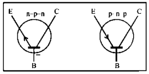
2.8.1. Action of n-p-n Transistor:
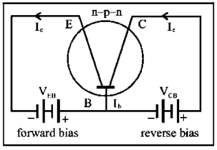
Fig. mentions that, the n-type emitter will be forward biased when connected it to \[-ve\] pole of \[{{V}_{EB}}\](emitter-base battery) and n-type collector will be reverse biased when connected it to \[+ve\] pole of \[{{V}_{CB}}\](collector-base battery).
The majority carriers (\[{{e}^{-}}\]) in emitter will be repelled towards base because of the forward bias. The base will be having holes as majority carriers but their number density is small because it is doped very lightly (\[5%\]) when we compare to emitter and collector. Because of the probability of \[{{e}^{-}}\] and hole combination in base will be small. Most of \[{{e}^{-}}\] (\[95%\]) cross into collector region where they will be swept away by \[+ve\] terminal of battery \[{{V}_{CB}}\].
In corresponds to each electron that is taken by collector, an electron will enter the emitter from \[-ve\] pole of collector – base battery.
When \[{{I}_{e}},{{I}_{b}},{{I}_{c}}\] be emitter, base and collector current respectively then by the use of Kirchoff’s first law, we can say that,
\[{{I}_{e}}={{I}_{b}}+{{I}_{c}}\]
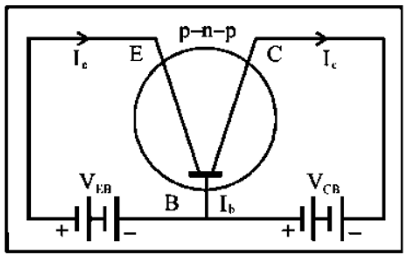
2.8.2. Action of p–n–p Transistor:
The p–type emitter will be forward biased when we connect it to \[+ve\] pole of emitter–base battery and p–type collector will be reverse biased when it is connected to \[-ve\] pole of collection - base battery. Here, majority carriers in emitter, that is holes will be repelled towards base because of forward bias. As base is lightly doped, it will be having low number density of \[{{e}^{-}}\]. If hole enters base region, then only \[5%\] of \[{{e}^{-}}\] and hole combination will be occurring. Most of the holes will be reaching the collector and are swept away by \[-ve\] pole of \[{{V}_{CB}}\] battery.
2.9. Common base Amplifier:
Here, base of the transistor will be common to both emitter and collector.
(a) Amplifier circuit by the use of n-p-n transistor: The emitter will be forward biased by the use of emitter bias battery (Vcc) and because of this, resistance of output circuit will be large.
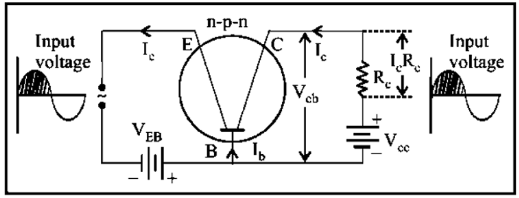
Low input voltage will be applied across emitter – base circuit and amplified circuit will be received across collector - base circuit. When\[{{I}_{e}},{{I}_{b}},{{I}_{c}}\] be the emitter, base and collector current then,
\[{{I}_{e}}={{I}_{b}}+{{I}_{c}}\]…\[(i)\]
If current \[{{I}_{c}}\] is flowing in collector circuit, a potential drop \[{{I}_{c}}{{R}_{c}}\] will be happening the resistance connected in collector - base circuit and base collector voltage will be,
\[{{V}_{cb}}={{V}_{cc}}-{{I}_{c}}{{R}_{c}}...(ii)\]
(b) Amplifier circuit by the use of p–n–p Transistor:
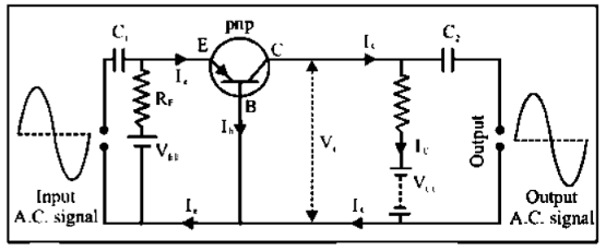
1. If the positive half cycle of input a.c. signal voltage is coming, it supports the forward biasing of the emitter–base circuit. Due to this, the emitter current increases and consequently the collector current increases.
2. As \[{{I}_{c}}\] increases, the collector voltage \[{{V}_{c}}\] decreases.
3. Since the collector is connected to the negative terminal of \[{{V}_{CC}}\] battery of voltage \[{{V}_{CB}}\], therefore, the reduction in collector voltage shows that the collector is becoming less negative. This represents that while positive half cycle of input a.c. signal voltage occurs, the output signal voltage at the collector will be also varying through the positive half cycle.
4. In the same way, when a negative half cycle of input a.c. signal voltage occurs, the output signal voltage at the collector also varies through the negative half cycle. Hence, the input signal voltage and the output collector voltage are in the same phase in common base transistor amplifier circuit.
2.10. Common Emitter Amplifier:
Amplifier Circuit by the Use of n–p-n Transistor:
1. The input (emitter base) circuit will be forward biased with battery \[{{V}_{BB}}\] of voltage \[{{V}_{EB}}\], and the output (collector-emitter) circuit will be reversed biased with battery \[{{V}_{CC}}\] of voltage \[{{V}_{CE}}\]. Because of this, the resistance of input circuit will be low and that of output circuit will be high. \[{{R}_{c}}\] will be a load resistance connected in collector circuit.
2. If a.c. signal voltage has not been applied to the input circuit but emitter base circuit being closed, assume that \[{{I}_{e}},{{I}_{b}}\] and \[{{I}_{c}}\] be the emitter current, base current and collector current respectively. Then in accordance to Kirchhoff’s first law
\[{{I}_{e}}={{I}_{b}}+{{I}_{c}}\]
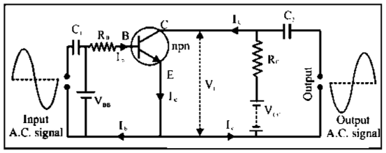
3. If the positive half cycle of input a.c. signal voltage is considered, it will be supporting the forward biasing of the emitter-base circuit. Because of this, the emitter current will be increasing and as a result the collector current will get increased. Because of which, the collector voltage \[{{V}_{c}}\] will be decreased.
4. Since the collector has been connected to the positive terminal of \[{{V}_{CE}}\] battery, therefore the reduction in voltage at the collector means the collector will become less positive, which shows that negative in accordance to initial value. This shows that while positive half cycle of input a.c. signal voltage occurs, the output signal voltage at the collector will be varying through a negative half cycle.
5. If negative half cycle of input a.c. signal voltage is considered, it will be opposing the forward biasing of emitter-base circuit, because of this the emitter current will be decreasing and therefore collector current will get decreased; As a result, the collector voltage \[{{V}_{c}}\] gets increased. That is, the collector will be more positive. This shows that when the negative half cycle of input a.c. signal voltage occurs, the output signal voltage will be varying through positive half cycle.
2.11. Common Base Amplifier:
A.c. Current Gain: This can be explained as the ratio of variation in collector current as fixed collector voltage. It is represented by \[{{\alpha }_{ac}}\]
\[{{\alpha }_{ac}}=\left( \frac{\Delta {{I}_{c}}}{\Delta {{I}_{e}}} \right)\]
\[\left[ {{V}_{CB}}=\text{ const}\text{.} \right]\]
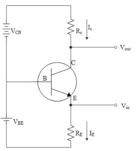
Voltage Gain: This can be referred as the ratio of variation in output voltage to the variation in input voltage. It can be represented as \[A\].
\[{{\text{A}}_{\text{v}}}\text{=}\frac{\left( \text{ }\!\!\Delta\!\!\text{ }{{\text{I}}_{\text{c}}} \right){{\text{R}}_{\text{out}}}}{\left( \text{ }\!\!\Delta\!\!\text{ }{{\text{I}}_{\text{e}}} \right){{\text{R}}_{\text{in}}}}\text{=}\frac{\text{ }\!\!\Delta\!\!\text{ }{{\text{I}}_{\text{c}}}}{\text{ }\!\!\Delta\!\!\text{ }{{\text{I}}_{\text{e}}}}\text{ }\!\!\times\!\!\text{ }\frac{{{\text{R}}_{\text{out}}}}{{{\text{R}}_{\text{in}}}}\]
Or \[{{\text{A}}_{\text{v}}}\text{=}{{\text{ }\!\!\alpha\!\!\text{ }}_{\text{AC}}}\text{ }\!\!\times\!\!\text{ resistance gain,}\]
Where \[\frac{{{\text{R}}_{\text{out}}}}{{{\text{R}}_{\text{in}}}}\] can be referred as resistance gain.
Power Gain: This can be explained as the ratio of variation in output power
to the variation in input power. Hence,
\[\text{a}\text{.c}\text{. power gain=}\frac{\text{change in output power}}{\text{change in input power}}=\frac{\left( \Delta {{I}_{c}} \right){{R}_{out}}}{\left( \Delta {{I}_{e}} \right){{R}_{in}}}\]
\[=\frac{\Delta {{I}^{2}}_{c}}{\Delta {{I}^{2}}_{e}}\times \frac{{{R}_{out}}}{{{R}_{in}}}\]
Or \[\text{a}\text{.c}\text{. power gain=}{{\alpha }^{2}}_{ac}\times \text{ resistance gain}\]
2.12. Common Emitter Amplifier:
A.c. Current Gain: The ratio of the variation in collector to the variation in base current can be defined as a.c current gain. It is represented as \[{{\beta }_{ac}}\].
Hence,
\[{{\beta }_{ac}}=\left( \frac{\Delta {{I}_{c}}}{\Delta {{I}_{b}}} \right)\text{ }[{{V}_{ce}}=\text{ const}\text{. }\!\!]\!\!\text{ }\]
The value of this quantity is quite large as compared to \[1\] and it lies between \[15\] to \[50\].
Voltage Gain: The ratio of the variation in output voltage to the
variation in input voltage can be referred as voltage gain. It is represented as \[A\].
\[{{\text{A}}_{\text{v}}}\text{=}\frac{\left( \text{ }\!\!\Delta\!\!\text{ }{{\text{I}}_{\text{c}}} \right)\text{ }\!\!\times\!\!\text{ }{{\text{R}}_{\text{out}}}}{\left( \text{ }\!\!\Delta\!\!\text{ }{{\text{I}}_{\text{b}}} \right)\text{ }\!\!\times\!\!\text{ }{{\text{R}}_{\text{in}}}}\text{=}\frac{\text{ }\!\!\Delta\!\!\text{ }{{\text{I}}_{\text{c}}}}{\text{ }\!\!\Delta\!\!\text{ }{{\text{I}}_{\text{b}}}}\text{ }\!\!\times\!\!\text{ }\frac{{{\text{R}}_{\text{out}}}}{{{\text{R}}_{\text{in}}}}\]
Or
\[{{\text{A}}_{\text{v}}}\text{=}{{\text{ }\!\!\beta\!\!\text{ }}_{\text{ac}}}\text{ }\!\!\times\!\!\text{ resistance gain}\text{.}\]
A.c. Power Gain: The ratio of the variation in output power to the variation in input power can be defined as A.c power gain.
\[\text{a}\text{.c}\text{. power gain=}\frac{\text{change in output power}}{\text{change in input power}}=\frac{\left( \Delta {{I}_{c}} \right){{R}_{out}}}{\left( \Delta {{I}_{b}} \right){{R}_{in}}}\]
Or \[\text{a}\text{.c}\text{. power gain=}{{\beta }^{2}}_{ac}\times \text{ resistance gain}\].
2.13. Relation Between \[\alpha \] and \[\beta \]:
In the case of both the types of amplifier, we will be having
\[{{i}_{e}}={{i}_{b}}+{{i}_{c}}\]
Divide both sides of the equation given above by \[{{I}_{c}}\], we will obtain,
\[\frac{{{i}_{e}}}{{{i}_{c}}}=\frac{{{i}_{b}}}{{{i}_{c}}}+1\]
\[\therefore \frac{\text{1}}{\text{ }\!\!\alpha\!\!\text{ }}\text{=(}\frac{\text{1}}{\text{ }\!\!\beta\!\!\text{ }}\text{)+1 or }\frac{\text{1}}{\text{ }\!\!\beta\!\!\text{ }}\text{=(}\frac{\text{1}}{\text{ }\!\!\alpha\!\!\text{ }}\text{)-1=}\frac{\text{(1- }\!\!\alpha\!\!\text{ )}}{\text{ }\!\!\alpha\!\!\text{ }}\]
Or \[\text{ }\!\!\beta\!\!\text{ =}\frac{\text{ }\!\!\alpha\!\!\text{ }}{\text{(1- }\!\!\alpha\!\!\text{ )}}\]
Similarly,
The relation of \[\alpha \] in terms of \[\beta \],
\[\alpha =\frac{\beta }{1+\beta }\]
3. Analog Signals:
Analog signal can be defined as the signals which is varying continuously with respect to time. A typical analog signal has been represented in the diagram below. Circuit which has been used for the generation of analog signal can be defined as the analog electronic circuit.
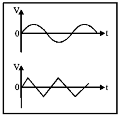
4. Digital Signals:
Signals which are having either of the two levels, \[0\] or \[1\], can be defined as digital signals.
5. Logic Gates:
A gate can be explained such that a digital circuit which is either stopping a signal or permitting it to pass through it. A logic gate will be an electronic circuit which will be creating logical decisions. Logic gate will be having one or more inputs but only one output. Logic gates are considered as the basic building blocks for every digital systems. Variables used at the input and output will be \[1's\] and \[0's\]. The three basic logic gates are mentioned below:
(i) OR gate
(ii) AND gate
(iii) NOT gate
5.1. OR Gate:
OR gate can be considered as an electronic equipment that is combining \[A\] and \[B\] for providing \[Y\] as output. Two inputs are \[A\] and \[B\] and output is \[Y\] in this figure. In Boolean algebra OR is shown as \[+\].
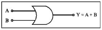
Truth Table: This can be defined as a table which is providing an output state for all possible input combinations.
Logic operations of OR gate has been provided in its truth table for all possible input combinations.
5.2. AND Gate:
There are two or more inputs and one output in an AND gate. In Boolean algebra AND has been denoted as a dot (.).
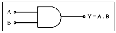
Truth Table
5.3. NOT Gate:
NOT gate can be considered as an electronic device which is having one input and one output. This circuit will be known as the same as the output is NOT the similar one as input.
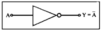
Boolean expression for NOT gate is \[Y=\overline{A}\].
Truth Table:
5.4. NOR Gate:
A NOR gate will have two or more inputs and only one output. Here, NOR gate is a NOT-OR gate actually. When a NOT gate has been connected at the output of an OR gate, we will be getting NOR gate as represented in the diagram below and its truth table in table.
Truth Table:
Boolean expression for NOT gate will be \[Y=\overline{A+B}\] and this can be read as \[Y\] equals \[A\] OR \[B\] negated. A NOR function will be the reverse of OR function.
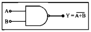
Truth Table:
5.5. NAND Gate:
A NAND gate will be having two or more inputs and only one output. A NAND gate is actually a NOT–AND gate. When a NOT gate has been connected at the output of a AND gate, we will be getting NAND gate as represented in the diagram and its truth table has been shown in table.
Boolean expression for NAND gate, will be \[Y=\overline{A\cdot B}\] and is read as \[Y\] equals \[\text{A}\]and \[\text{B}\] negated.
Logical symbol of the NAND gate has been represented in the diagram and its truth table in table.
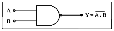
Truth Table:
Similar to NOR gate, NAND gate will also be useful to realize all basic gates: OR, AND and NOT. Therefore it is also called as Universal Gate.
Universal Gate:
A universal gate can be defined as a logic gate which can be used to perform any Boolean function with no utilization of any other type of logic gate. Examples of universal gates are NOR gate and NAND gate.
Integrated Circuits:
The conventional process of creating circuits will be to choose components such as transistors, diodes, R, L, C etc., and connect them using soldering wires in the required manner. The commonly used technology will be the Monolithic Integrated Circuit.
These kinds of circuits contain logic gates. When we depend upon the level of integration (that is, the number of circuit components or logic gates), the ICs can be defined as Small Scale Integration, SSI (logic gates < 10), Medium Scale Integration, MSI (logic gates < 100), Large Scale Integration, LSI (logic gates < 1000) and Very Large Scale Integration, VLSI (logic gates > 1000).
Class 12 Physics Revision Notes for Chapter 14 - Semiconductor Electronic: Material, Devices And Simple Circuits
Class 12 Notes Semiconductor Electronics
Some devices like vacuum diodes were manufactured and used to control the flow of electrons in a circuit before the discovery of transistors. Nowadays, the usage of these devices is obsolete.
These devices were bulky, spent high power, functioned at high voltages. Also, these devices had limited life and reliability.
Physicists had concluded in the year of 1930 that the solid-state semiconductors and their junction presented the opportunity of monitoring the flow of charge exports through them. The modern solid-state semiconductors are known as LEDs, otherwise light-emitting diodes.
These LEDs ingest low power in a very few amounts, operate at low voltages, hold a durable life, and high reliability.
We Are Going to Study About These Following Concept in Chapter 12:
Elementary ideas of semiconductor Physics
Semiconductor devices (bipolar junction transistor and junction diodes)
Semiconductors and its applications
CBSE Class 12 Physics Notes Chapter 14 Semiconductor Electronic Material Devices and Simple Circuits
In order to define the Semiconductors, these are used in solid-state electronic devices such as transistors, diodes, etc. Semiconductors are acted as the fundamental core materials.
It is our complete freedom to choose any of the materials like metal, semiconductor, or insulator. These elements can be treated as the semiconductors such as Ge, Si, or compounds like CdS or GaAs.
Semiconductor Devices Class 12 Notes PDF
In this chapter, students are going to face the questions about calculating the output frequency of a half-wave and full-wave rectifier. Also, they have to answer some questions on finding the input signal and base current of a CE-Transistor amplifier.
In Semiconductor Devices Class 12 Notes PDF, Vedantu can offer help to the students to find out the output AC signal if two amplifiers are connected in series. When a condition arises about the fabrication of a p-n photodiode, will it detect wavelengths? These kinds of questions are also given in the notes.
There are some other practice questions based on this chapter that contain finding several holes and electrons in atoms of silicon, Indium, and arsenic.
In this way, chapter 14 of semiconductor electronic material devices and simple circuits will be covered with concepts as well as questions and answers.
NCERT Semiconductor Devices Class 12 Notes PDF
The following subtopics are present in Semiconductor Class 12 Notes PDF:
1. Introduction
2. Classification of Metals, Conductors, And Semiconductors
3. Extrinsic Semiconductor
4. Intrinsic Semiconductor
5. p-n Junction
a. p-n Junction formation
6. Semiconductor Diode
a. p-n junction diode under reverse bias
b. p-n junction diode under forwarding bias
7. Application of Junction Diode as A Rectifier
8. Special Purpose P-n Junction Diodes
a. Zener diode
b. Optoelectronic junction devices
9. Junction Transistor
a. Transistor: structure and action
b. Basic transistor circuit configurations and transistor characteristics
c. Transistor as a device
d. Feedback amplifier and transistor oscillator
e. Transistor as an Amplifier (CE-Configuration)
10. Digital Electronics and Logic Gates
a. Integrated Circuits
b. Logic gates
Download CBSE Class 12 Physics Notes Semiconductor Electronic Material Devices and Simple Circuits PDF
Interested students can download the CBSE Semiconductor Electronics Class 12 Notes in PDF format from our website. You can also download the same from Vedantu app.
Why Choose Vedantu for CBSE Physics Semiconductor Electronics Class 12 Notes?
Vedantu has provided some fabulous features about the CBSE Class 12 Physics provided. The following points can definitely give you a good idea to choose the Vedantu as your study program partner.
1. Vedantu has uploaded the pdf files on their website that contain CBSE Class 12 Physics notes. These notes are well-systematized and supportive for easy learning.
2. Some particular experts do their hard work to prepare the CBSE Class 12 Physics notes. This feature can also benefit the students very much.
3. Students are requested to practice on the model papers of the CBSE Class 12 Physics notes regularly. It can give them the ability to secure the best marks in their board exams.
4. In the Vedantu learning app, the CBSE Class 12 Physics PDF files comprise arithmetical problems along with the proper concepts. All of them are explained precisely by giving perfect clarification to each question.
Related Physics Class 12 Links for Semiconductors Class 12 Notes
Semiconductor Devices & Communication System Related Important Links
It is a curated compilation of relevant online resources that complement and expand upon the content covered in a specific chapter. Explore these links to access additional readings, explanatory videos, practice exercises, and other valuable materials that enhance your understanding of the chapter's subject matter.
Class 12 Study Materials Important Links
Find a curated selection of study resources for Class 12 subjects, helping students prepare effectively and excel in their academic pursuits along with Semiconductors Class 12 Notes.
Conclusion
The Semiconductors Class 12 Notes provide a comprehensive resource for students delving into the intricate world of semiconductor physics. With detailed explanations, illustrative diagrams, and practical examples, these notes offer invaluable support for CBSE Physics students navigating Chapter 14. Whether preparing for exams or seeking a deeper understanding of semiconductor principles, this free PDF download serves as a reliable companion on the journey to academic success.
FAQs on Semiconductor Class 12 Notes CBSE Physics Chapter 14 (Free PDF Download)
1. What Are the Methods to Do Well in the CBSE Board Exam?
Securing good marks in the CBSE board exam is quite simple. All you require is a precise plan. Scholars have to give their best on every subject and cover the syllabus within the perfect time.
Also, students must be clear about the perceptions of exact subjects like Physics, Chemistry, mathematics, and other literature subjects. The continuous practice of mock tests and practice papers can also help the students.
2. Explain that Silicon is a Semiconductor.
The main reason is that Silicon is the vital component of sand, and for this purpose, it is less expensive than other essential semiconductor materials. Before the use of Silicon, germanium was used as a semiconductor.
3. Describe the Reason for the Usage of Gold in the Motherboard.
Gold is recognized as a marvellous conductor of electricity. This is the importance of gold as it is widely used among much electrical equipment like RAM. In RAM, the gold is utilized as a coating.
4. What is a semiconductor in Chapter 14 of Physics Semiconductor Notes PDF?
Chapter 14 of Class 12 Physics is “Semiconductor Electronic: Material, Devices And Simple Circuits”. Semiconductors are materials characterised by conductivity ranges that lie somewhere between conductors (usually metals) and nonconductors (insulators) (such as most ceramics). Semiconductors generally exhibit the composition of pure elements like silicon and germanium, as well as compounds like gallium arsenide and cadmium selenide. They have multiple uses across different domains and hence are of great importance in the electrical and electronics industry. To know more about semiconductors, refer to the notes by visiting the link NCERT notes for Class 12 Physics.
5. What are electronic devices in Chapter 14 of Physics Class 12?
If you're looking for anything to regulate the flow of electrons or other electrically charged particles through circuits, you're looking for an electronic device. Electronics is the branch of science that deals with electrons' emission and movement as well as their control in a vacuum or matter. Many industries rely heavily on electronic devices to handle data and communicate. Digitised information processing is made feasible by electronic devices that may be used as switchboards. Download the Vedantu app and learn more about electronic devices.
6. How can I download Class 12 Physics Chapter 14 Semiconductor Notes PDF?
To download the Semiconductor Notes PDF of NCERT Class 12 Physics Chapter 14, follow these steps -
Visit the page-Revision Notes for chapter 14 of Class 12 Physics.
The webpage with Vedantu’s notes for Class 12 Physics Chapter 14 will open. You can use this link to access the Class 12 Chapter 14 revision notes.
To download this, click on the Download PDF button, and you can view the notes offline free of cost.
Feel free to check the other subjects or topics whose solutions you might want to refer to on the Vedantu site.
7. How do semiconductors work?
A semiconductor is a material that combines the properties of a conductor and an insulator. Conductors are high-conductivity materials that enable charge to flow when a voltage is applied, whereas insulators do not. Semiconductors may behave as both an insulator and a conductor when needed. As the temperature rises, its resistivity decreases. Metals, on the other hand, react oppositely. The study of these semiconductors is extremely necessary due to their applications across multiple domains.
8. Where do we use semiconductors?
Semiconductors are used in the CPUs that run personal computers. Semiconductors find their usage in a wide variety of digital consumer devices such as smartphones, digital cameras, televisions, washing machines, refrigerators, and LED bulbs. Semiconductors are also used in the production of diodes, transistors, and integrated circuits, among multiple other types of electronic devices. Because of their compactness, dependability, power efficiency, and low cost, semiconductors have found widespread use. They have multiple uses across different domains. To revise all the important things, students can download the free PDF of revision notes from the Vedantu website (vedantu.com).