
Monolithic Use of Inert Gas for Highly Transparent and Conductive Indium Tin Oxide Thin Films

1
Environment and Sustainability Institute, University of Exeter, Penryn Campus, Cornwall TR10 9FE, UK
2
Department of Physics and Renewable Energy, College of Science and Humanities-Jubail, Imam Abdulrahman Bin Faisal University, Jubail 35811, Saudi Arabia
3
Physics Department, University of Hafr Al Batin, Al Jamiah, Hafar Al Batin 39524, Saudi Arabia
*
Author to whom correspondence should be addressed.
Nanomaterials 2024, 14(7), 565; https://doi.org/10.3390/nano14070565
Submission received: 12 February 2024
/
Revised: 17 March 2024
/
Accepted: 20 March 2024
/
Published: 24 March 2024
(This article belongs to the Topic Advances in Functional Thin Films)
Abstract
:Due to its excellent electrical conductivity, high transparency in the visible spectrum, and exceptional chemical stability, indium tin oxide (ITO) has become a crucial material in the fields of optoelectronics and nanotechnology. This article provides a thorough analysis of growing ITO thin films with various thicknesses to study the impact of thickness on their electrical, optical, and physical properties for solar-cell applications. ITO was prepared through radio frequency (RF) magnetron sputtering using argon gas with no alteration in temperature or changes in substrate heating, followed with annealing in a tube furnace under inert conditions. An investigation of the influence of thickness on the optical, electrical, and physical properties of the films was conducted. We found that the best thickness for ITO thin films was 100 nm in terms of optical, electrical, and physical properties. To gain full comprehension of the impact on electrical properties, the different samples were characterized using a four-point probe and, interestingly, we found a high conductivity in the range of 1.8–2 × 10⁶ S/m, good resistivity that did not exceed 1–2 × 10⁻⁶ Ωm, and a sheet resistance lower than 16 Ω sq−1. The transparency values found using a spectrophotometer reached values beyond 85%, which indicates the high purity of the thin films. Atomic force microscopy indicated a smooth morphology with low roughness values for the films, indicating an adequate transitioning of the charges on the surface. Scanning electron microscopy was used to study the actual thicknesses and the morphology, through which we found no cracks or fractures, which implied excellent deposition and annealing. The X-ray diffraction microscopy results showed a high purity of the crystals, as the peaks (222), (400), (440), and (622) of the crystallographic plane reflections were dominant, which confirmed the existence of the faced-center cubic lattice of ITO. This work allowed us to design a method for producing excellent ITO thin films for solar-cell applications.
1. Introduction
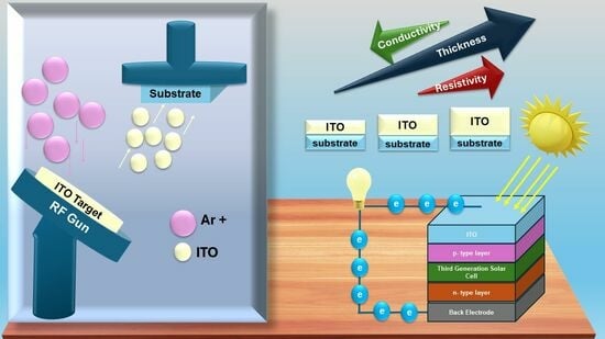
Transparent conducting oxide (TCO) materials are widely used to transmit light through materials and conduct electricity. To produce these materials, metal oxides are used, which include tin oxide (SnO2), aluminum oxide (Al2O3), indium oxide (In2O3) [1], and zinc oxide (ZnO) [2,3]. There are many uses and applications of TCOs, such as display devices like flat-panel screens and touchscreens [4]; smart windows, in which the transparency can be controlled through applying a voltage and, hence, the heat and light transmitted through the window can be controlled [5]; and optoelectronic devices such as light-emitting diodes (LEDs) and photodetectors [6]. ITO films are of crucial importance in optoelectronic devices and solar cells. ITO is mainly used as the front electrode in photovoltaic applications [7] due to its high conductivity and transparency ranges, which make it a favorable choice for fabrication. Several studies have investigated the different properties of ITO and how they can be optimized using different growth techniques and conditions. In particular, in third-generation solar cells like perovskites and dye-sensitized solar cells, several attempts have been made to increase the efficiency of lab-built ITO to be used as a front electrode through different approaches. Although ITO has many optical, electrical, and physical advantages in the field of optoelectronic devices and photovoltaics, the high manufacturing costs and scarcity of indium and tin supplies hinder the long-term viability and scalability of its usage in third-generation solar cells.
The growth technique can contribute to material savings through reducing the amount of wasted material during the synthesis process. Radio frequency (RF) magnetron sputtering is a favored method for the growth of ITO films, as it provides high uniformity and precision when it comes to the microstructure growth and the ratios of indium and tin, which can be accurately specified for the sputtering targets. Unlike liquid and chemical approaches to creating ITO, which create a large amount of wasted materials, RF magnetron sputtering can create thousands of highly transparent and uniform thin films using one sputtering target. Many studies have focused on the creation of ITO thin films with RF magnetron sputtering. In a study by Vinh Ai Dao et al. [8], they heated the substrates in the deposition process and used an oxygen flow. Their results showed proper ITO parameters and, when they used a temperature of 200 °C, the heterojunction silicon solar-cell efficiency reached 16%. In another study by M.G. Sousa et al. [9], they compared their created ITO glass with and without the use of hydrogen pressure within the chamber and with only argon but an RF power of 250 W. This also resulted in adequate properties for the ITO to be used in solar-cell applications. In a study by F. Kurdesau et al. [10], they used oxygen in the chamber alongside argon. Another recent study by Amalraj P. A et al. [11] investigated the effects of the film thickness and RF power on the optical and electrical properties of ITO films. Shumin Y. et al. [12] prepared four different ITO targets in their lab with different crystallinities and studied the effects of the crystallinity of ITO targets on the properties of the ITO films. In the study of D. Kudryashov et al. [13], they found that, with argon gas, the best power at room temperature was only 50 W, and they tested a thickness of 100 nm with different parameters that resulted in the appropriate parameters for solar-cell applications. A study published after 2020 mostly tackled ITO growth within other layers (e.g., Cu) in RF magnetron sputtering [14]. Recent published studies focused on variations in power and growth temperature, using different gases or only argon gas (the latter was quite rarely used). For this reason, we studied indium tin oxide films grown using the radio frequency magnetron sputtering technique with varying thicknesses, in order to study the effect of thickness on the film’s properties using argon gas alone. Our approach had interesting results which contribute to the existing scientific literature.
2. Materials and Methods
2.1. Preparation of ITO Samples Using PVD
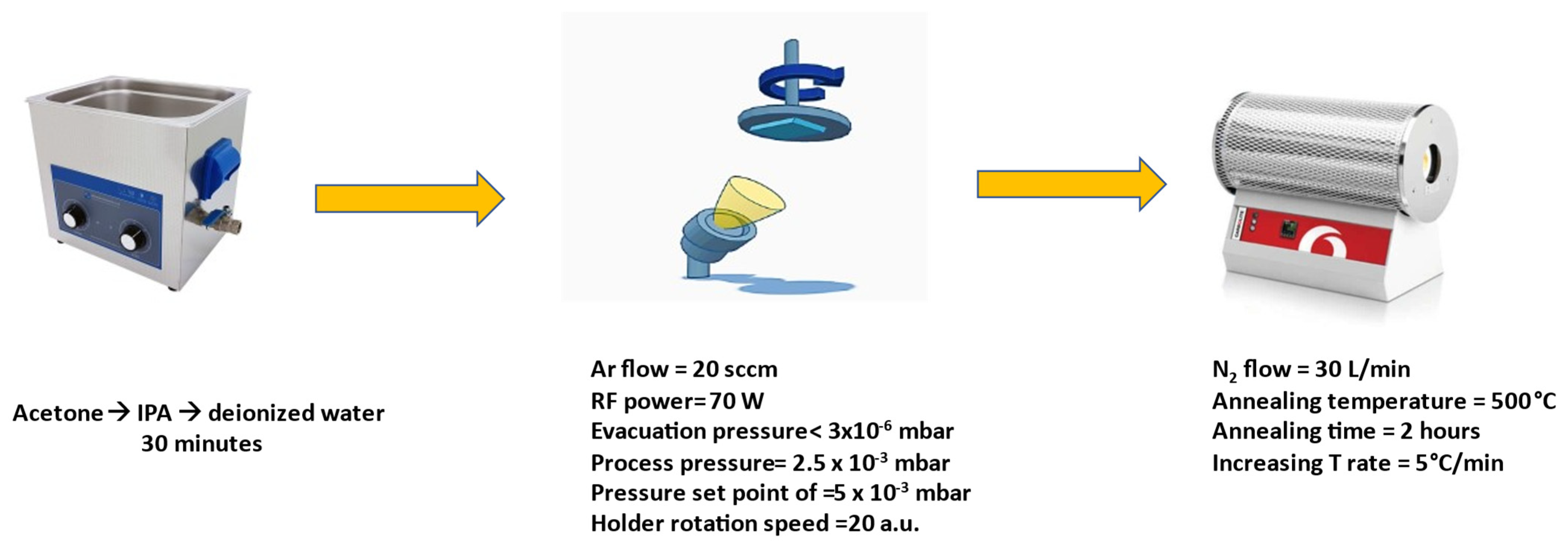
In this study, we used PVD (MiniLab ST060M R&D Magnetron Sputtering and Thermal Evaporation System, Moorfield Nanotechnology Limited. Cheshire, United Kingdom.) with load lock in the Environment and Sustainability Institute (ESI) solar lab to create films with different thicknesses using radio frequency sputtering. The ITO target was bought from Kurt J. Lesker, Sussex, United Kingdom, and had an indium to tin oxide ratio of 90/10 wt% In2O3/SnO2. The argon gas that was pumped to the chamber was of 99.99% purity and the silica low-iron glass substrates with a 4 mm thickness and 2 × 2 cm dimensions were obtained from Cornwall Glass Manufacturing, Plymouth, United Kingdom. The PVD was only run on the radio frequency magnetron sputtering system. The substrates were cleaned with acetone for 30 min, IPA for 30 min, and then deionized water for 30 min, all in an ultrasonic bath, and then dried in ambient air. The evacuation pressure of the chamber was less than 4 × 10⁻³ mbar. The ITO layers were manufactured in the radio frequency magnetron sputtering system chamber with a pressure set point of 5 × 10⁻³ mbar. The ITO sputtering during deposition was performed with an RF power of 70 W. The rotation speed for the substrate holder base was 20 a.u. and the Ar flow was 20 sccm. There was no increase in temperature on the base while growing the ITO films. Films with different thicknesses were grown: 50 nm, 100 nm, 150 nm, 200 nm, 250 nm, and 300 nm. As soon as the samples were manufactured, the samples were annealed at 500 °C for 2 h, with the temperature increasing at a rate of 5 °C per minute, in a tube furnace with a nitrogen gas flow (30 L/min) and they were left inside the furnace to cool to room temperature for another 2 h. Figure 1 illustrates the fabrication process with the different parameters used to grow the samples.
2.2. Characterization Techniques
A four-point probe was used to study the films’ electrical properties, as our main purpose was to find the thickness that resulted in the best electrical characteristics to be used as a front electrode. After choosing the best thickness in the context of optimal electrical properties, the optical characterization of the samples before and after annealing was performed through measuring the spectral dependence of the transmission (T(k)) of deposited ITO layers within the visible wavelength range (300–800 nm) using a spectrophotometer; through this, we calculated the absorbance and found the bandgap. Moreover, the samples’ physical properties were examined using X-ray diffraction (XRD) (Bruker D8 advanced XRD, Bruker, Billerica, MA, USA); atomic force microscopy (AFM) (Bruker Innova AFM, Bruker, Billerica, MA, USA), after staining the samples with a thin carbon layer; and later, scanning electron microscopy (SEM) (Tescan Vega 3, Tescan, Brno, Kohoutovice Czech Republic). We have included the before and after annealing measurements in order to understand the influence of annealing on the optical and electrical properties.
3. Results and Discussion
3.1. X-ray Diffraction Microscopy Measurements
Figure 2 shows the X-ray diffraction microscopy results for the films with different thicknesses before annealing. Almost all identifiable peaks lost some of their intensity, indicating that the ITO films had only a minimal amount of crystallinity before the annealing process. They had an amorphous quality for the most part. However, as the layer thickness increased, crystalline characteristics started to become more apparent.
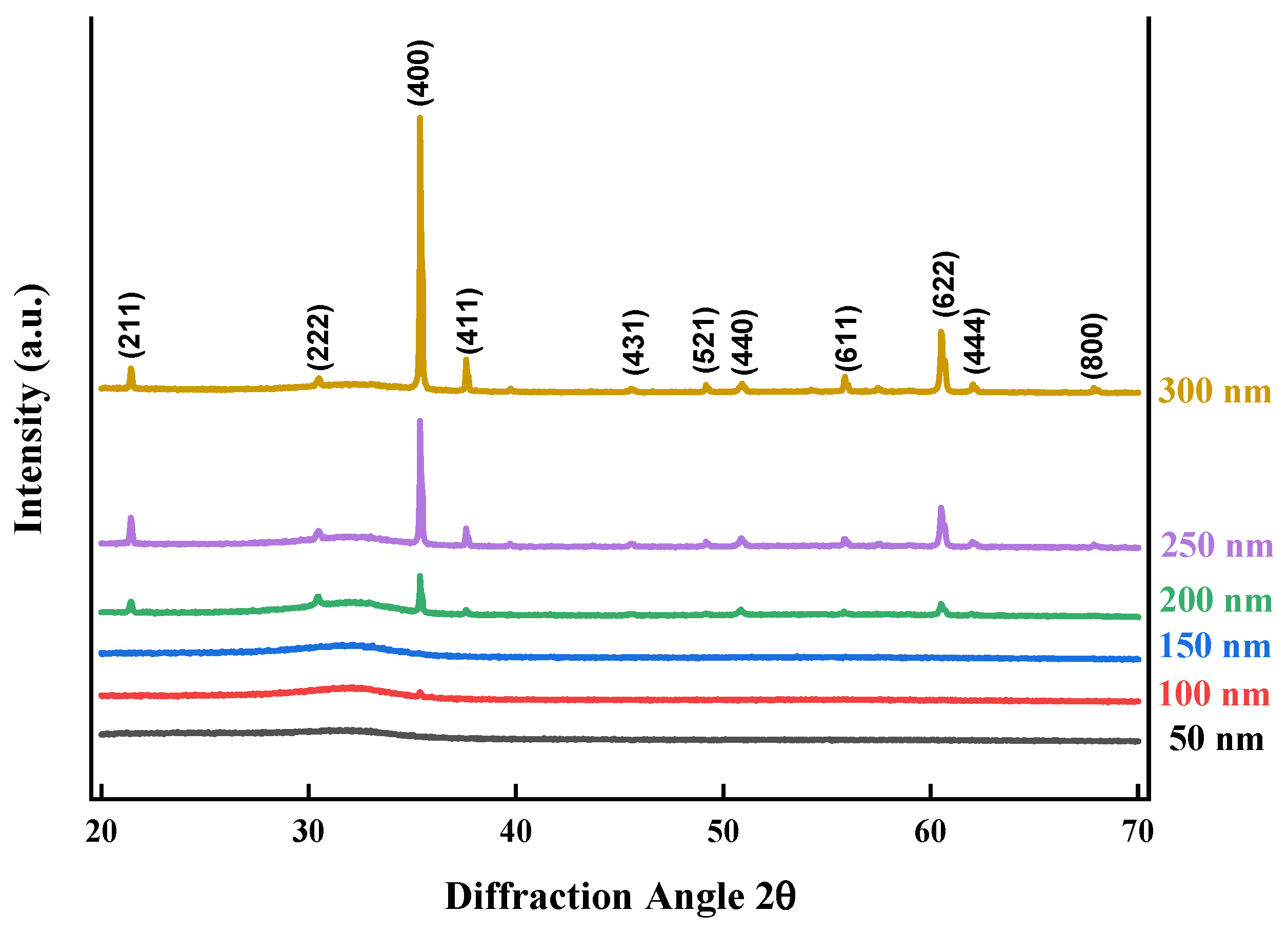
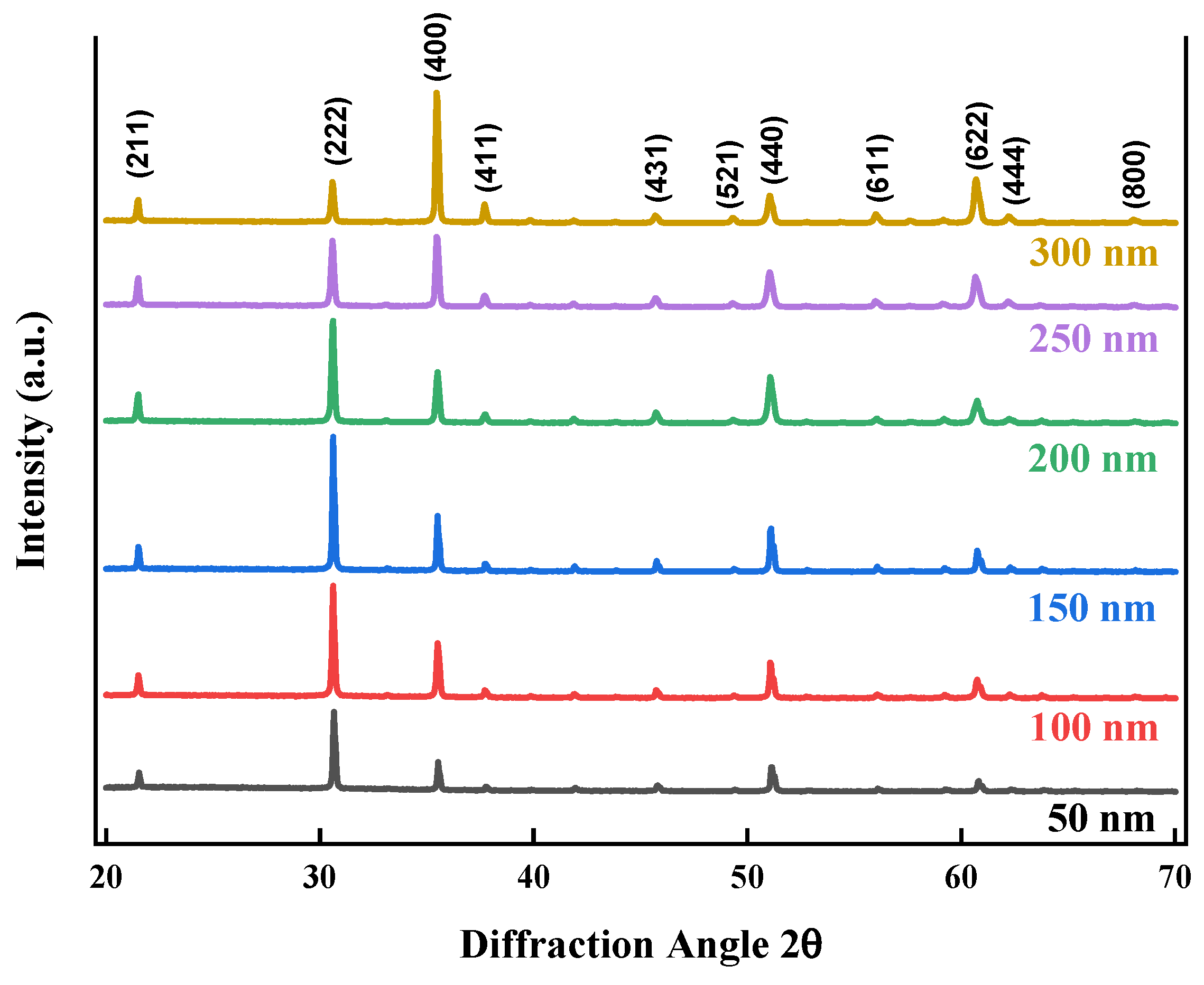
Following annealing, the X-ray diffraction patterns (Figure 3) were characterized by prominent peaks that unmistakably signified an increase in crystallinity. Because charge carriers are given organized paths within the lattice structure of ITO, facilitating charge mobility, this phenomenon has implications for improving conductivity. The (222), (400), (440), and (622) peaks are the prominent peaks for the faced-center cubic lattice of ITO crystallographic plane reflections [15,16,17]. The other peaks ((211), (411), (431), (521), (611), (444), and (800)) represent other planes’ reflections. As the thickness increased, the preferential crystal orientation changed to the (400) plane, as the grain strain increased towards this plane due to interstitial oxygen and indium vacancies.
The formation of strain results from both external elements like dislocations and extended defects within the crystalline lattice, as well as intrinsic point defects like vacancies and site disorder. The calculated lattice constants showed a notable agreement with known reference values (JCPDS card No. 71-2194) [18,19,20].
3.2. Atomic Force Microscopy
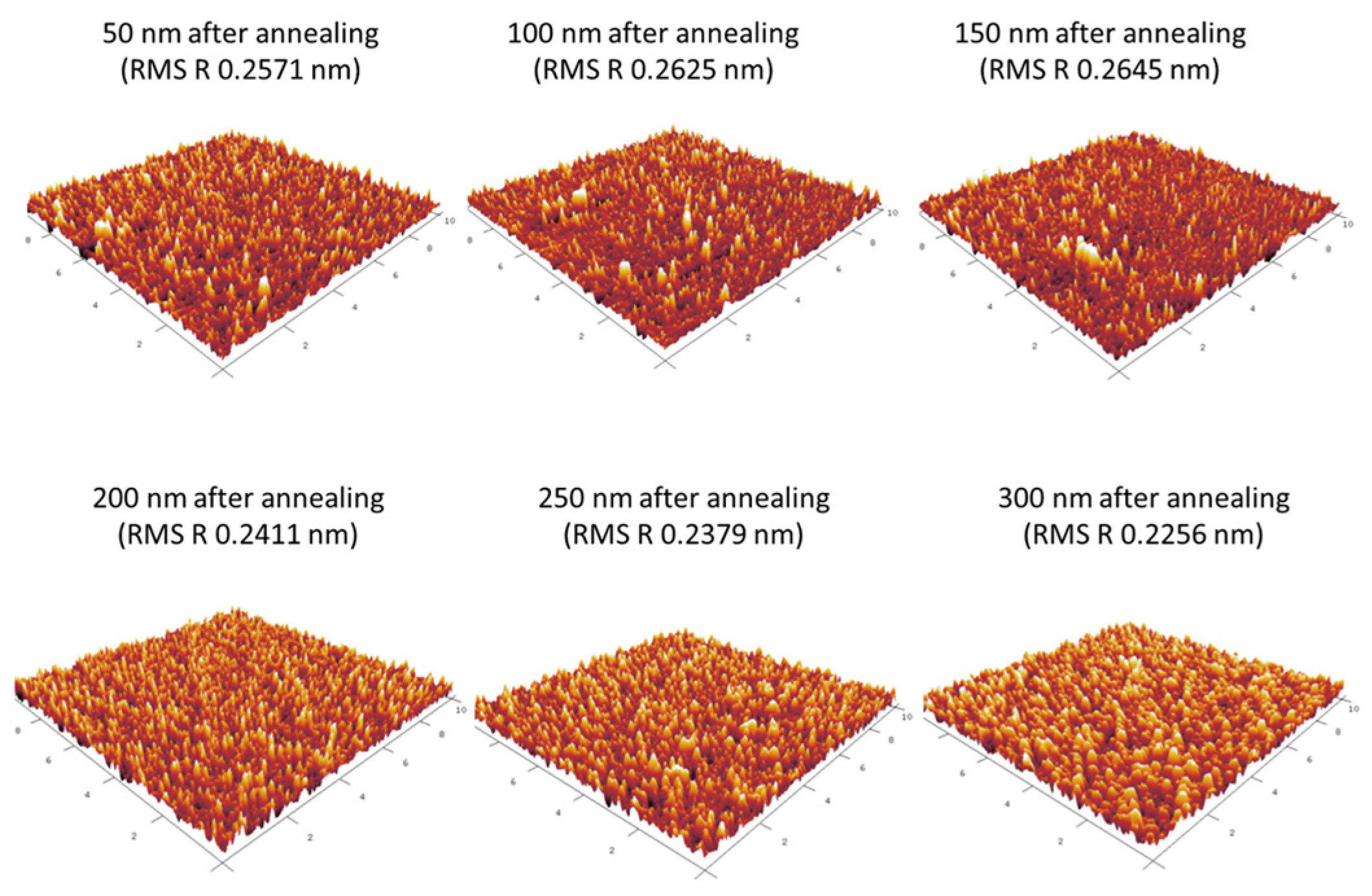
Atomic force microscopy (AFM) measurements were used to gain an understanding of the surface morphology of the indium tin oxide (ITO) films. The experiment aimed to gain a thorough understanding of the complex interactions between the films’ electrical characteristics and their underlying physical characteristics. The goal was to identify the relationship between the surface morphology and the distinctive qualities of the ITO films. Figure 4 shows a variety of unique samples of ITO films with different thicknesses. The images all have dimensions of 10 µm × 10 µm. During the analysis of these images, an important observation became apparent. The mean value of the peaks and valleys determined over the total surface area was measured and recorded as the average roughness. This helped us to identify broad differences in the properties of the overall profile height. The square root of the distribution of surface height is known as the root mean square roughness (RMS R), which is thought to be more sensitive than the average roughness. It displays the profile heights’ standard deviation. In particular, each film had RMS R values that were consistently lower than the nominal criterion of 0.3 nm. This overall pattern was a reliable predictor of the crystallinity of the ITO material under the growth conditions of our experiment [10,21,22]. Similar RMS roughness results were found using magnetron sputtering (0.546 nm) [23] and another deposition technique (0.293 nm) [24]. Alternatively, we can see higher RMS roughness values found by Rita M. Carvalho et al. [25] and others [26,27,28] ranging between 3.9 nm up to 24.8 nm. We attribute these rough ITO surfaces to high temperatures used during growth and annealing as, in one method, they used thermal evaporation which can induce the formation of indium oxide on the surface, creating a clear variation; to the lack of annealing in proper and inert conditions; to the deposition parameters that included the distance between the target and the substrate; and to the gas pressure in the chamber and the sputtering power. Our low RMS roughness values can be attributed to the growth method in a vacuum which hindered the oxidation and formation of rough layers in inert conditions. Moreover, using an inert gas in the annealing method contributed to smoother films as indium tends to oxidize at high temperatures which can increase the formation of random indium oxide particles on the surface.
A recognizable pattern was revealed through further analysis of the RMS R values. In particular, values between 0.2571 nm and 0.2645 nm gradually emerged as the ITO layer’s thickness rose, covering the thickness range of 50 nm to 150 nm. However, after reaching a thickness of 200 nm, this pattern underwent a noticeable shift. The measured RMS R levels started to decrease at this point, going from 0.2411 nm to 0.2256 nm for thicknesses of 200 nm to 300 nm. We suggest that this phenomenon can be attributed to the natural transition taking place at the surface, which signaled the emergence of a more refined and smooth ITO film and an increase in grain sizes. The changes shown in Figure 4 resemble this perceptible growth, as the sharpness of the tip ends changed to a more curved layout while simultaneously showing an expansion in the grain dimensions. From our experiment, we can conclude that all the layers had optimal RMS R values and crystalline amorphous structures, which tended to have higher roughness and lower conductivity values. With increased roughness, we acquired a higher conductivity which was a result of the tips being closer to one another which helped in the transitioning of charges on the surface.
In summary, our utilization of atomic force microscopy in the analysis of the ITO films unveiled the intricate relationships between surface morphology, crystallinity, and electrical conductivity [29]. The low RMS R values signified the crystalline nature of the ITO films that were produced under our experimental conditions. The distinct trend of roughness value vs. thickness further solidifies this notion.
3.3. Four-Point Probe
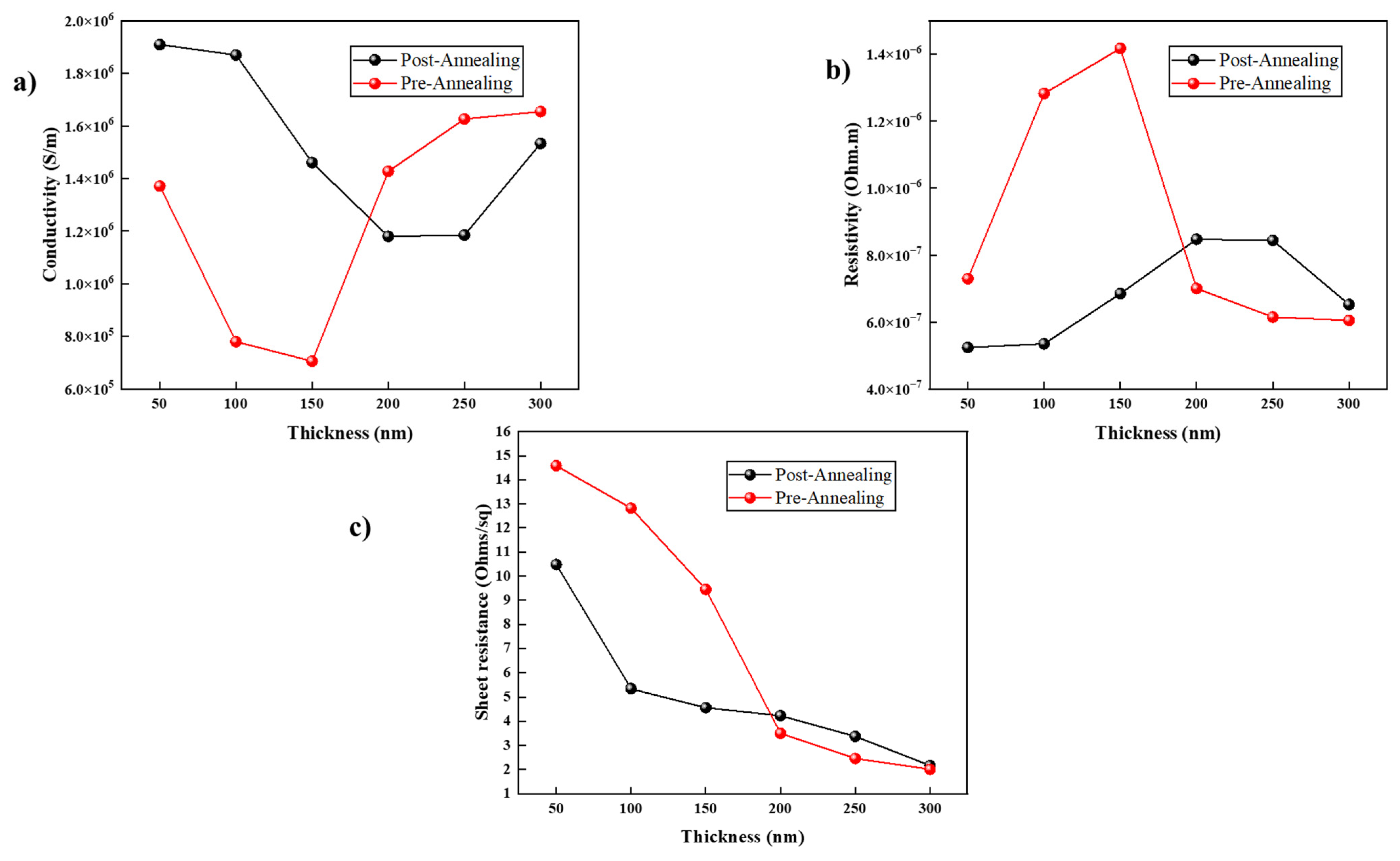
Figure 5a–c show the electrical properties of the ITO films with different thicknesses before and after annealing. It is essential to understand the electrical properties to determine the quality of the deposited ITO [30].
Conductivity is one of the most important properties of an ITO thin film layer in third-generation solar-cell devices. In our films, we found that the conductivity values decreased with increasing thickness and then sharply increased after reaching 200 nm prior to annealing; this can be explained as thicker layers having higher conductivity due to reduced scattering sites and defects. However, thick layers tend to have poor crystallinity. On the other hand, after annealing, the films showed better conductivity values as the grain size increased; therefore, there was less boundary scattering [8], and the recrystallization reduced crystal defects and improved the electron mobility in the lattice [31] with better results at 50 nm and 100 nm (between 1.8–2 × 10⁶ S/m). It is important to consider that the optimal conductivity for ITO used in optoelectronic materials and solar cells should not be less than 1 × 10⁴ S/m [32]. Another important property for suitable ITO thin films in third-generation solar-cell devices is resistivity. Figure 5b illustrates the resistivity of the ITO samples with different thicknesses before and after annealing. Prior to annealing, the films had a high resistivity which was attributed to the low mobility of charge carriers. Nevertheless, the resistivity was quite stable post-annealing and was in the optimal range for solar-cell applications. A good resistivity for ITO for solar-cell applications is less than 1–2 × 10⁻⁶ Ωm [33,34]. In our results, we obtained values of 4 × 10⁻⁷ to 9 × 10⁻⁷ Ωm, indicating an optimal quality for the created films. It can be seen that the lowest and optimal resistivity was measured from the films with thicknesses of 50 nm and 100 nm. Figure 5c shows the pre- and post-annealing sheet resistance values of the samples. Annealing plays an important role in reducing the values of sheet resistance [35] which, in turn, is highly affected by the resistivity and the thickness of the layer. From the figure, we can observe that annealing improved the sheet resistance (Rsh). Equation (1) links these variables together:
where ρ is the resistivity of the thin film and t is the thickness of the thin film. It is expected that with increased thickness, we will have lower sheet resistance values. Nonetheless, the lower sheet resistance of these samples was also associated with a slightly lower conductivity and higher resistivity. Therefore, the optimal thickness based on the electrical properties was 100 nm. We could also opt for 50 nm but the film with this thickness showed a high sheet resistance that might affect the layers grown on the ITO and the efficiency of the solar device. We can conclude that annealing plays an important role in the improvement of ITO thin films [36].
3.4. Scanning Electron Microscopy
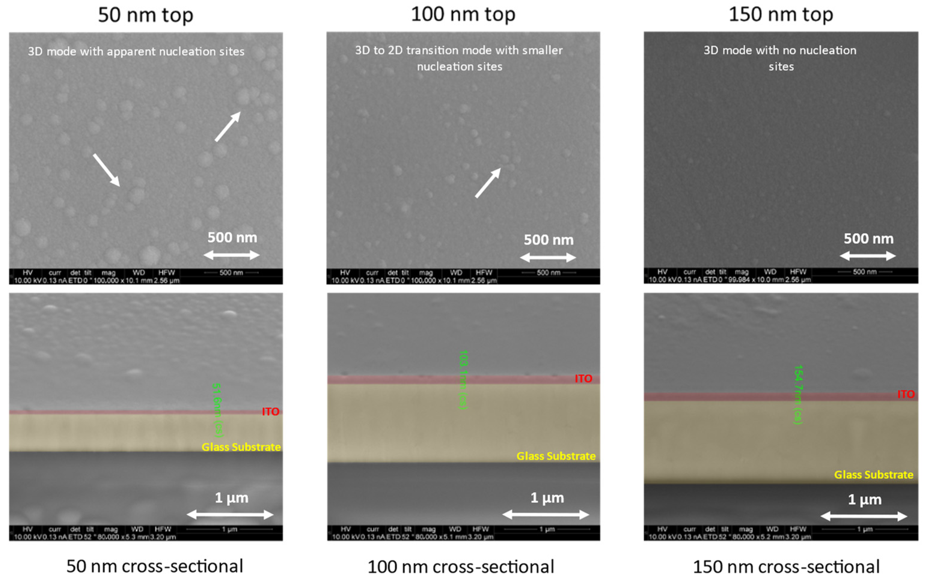
Scanning electron microscopy (SEM) was performed to confirm the actual thickness of each layer and to study the influence of the morphology on the optical, electrical, and mechanical properties of the films.
We can see, from the images in Figure 6 and measurements, that the thickness of the films was accurate; this suggests high-precision growth using the radio frequency magnetron sputtering machine: the 50 nm film was measured as 51.6 nm, the 100 nm film was measured as 103.1 nm, and the 150 nm film was measured as 154.6 nm. The analysis revealed a shared characteristic among all the films: a uniform surface structure composed of nucleation sites pointed by white arrows in the figure that decreased in size as the thickness increased; this is because the Volmer–Weber island growth mode shifted to a Frank–van der Merwe mode, which is a transition from a 3D growth mode to a 2D growth mode, when the thickness was increased and the nodes and clusters were transformed into layers. This smoothness, which was free from both empty spaces and fractures, created good conductivity as fractures can contribute to extremely irregular electrical voltages on the surface [37,38].
3.5. Optical Properties
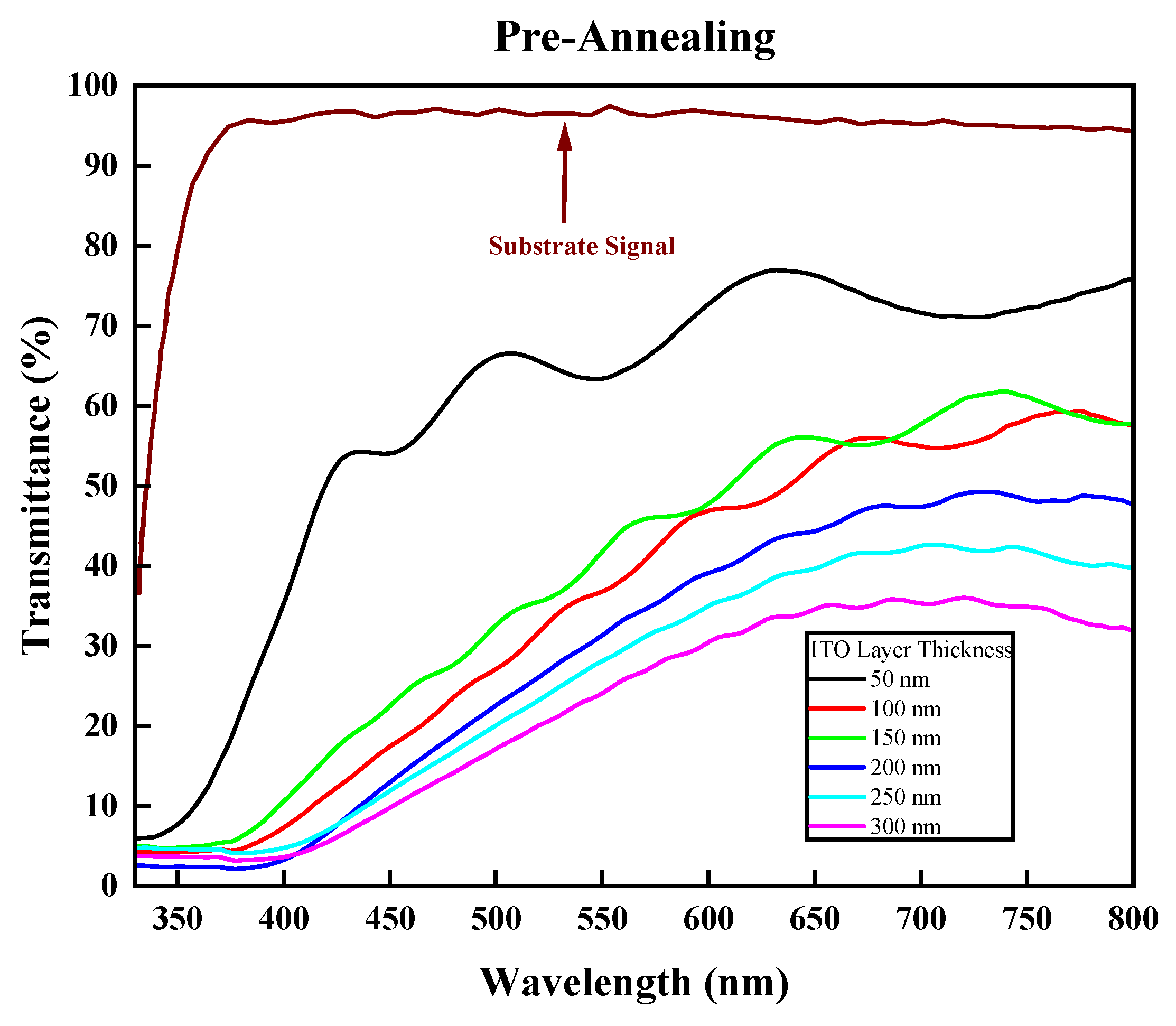
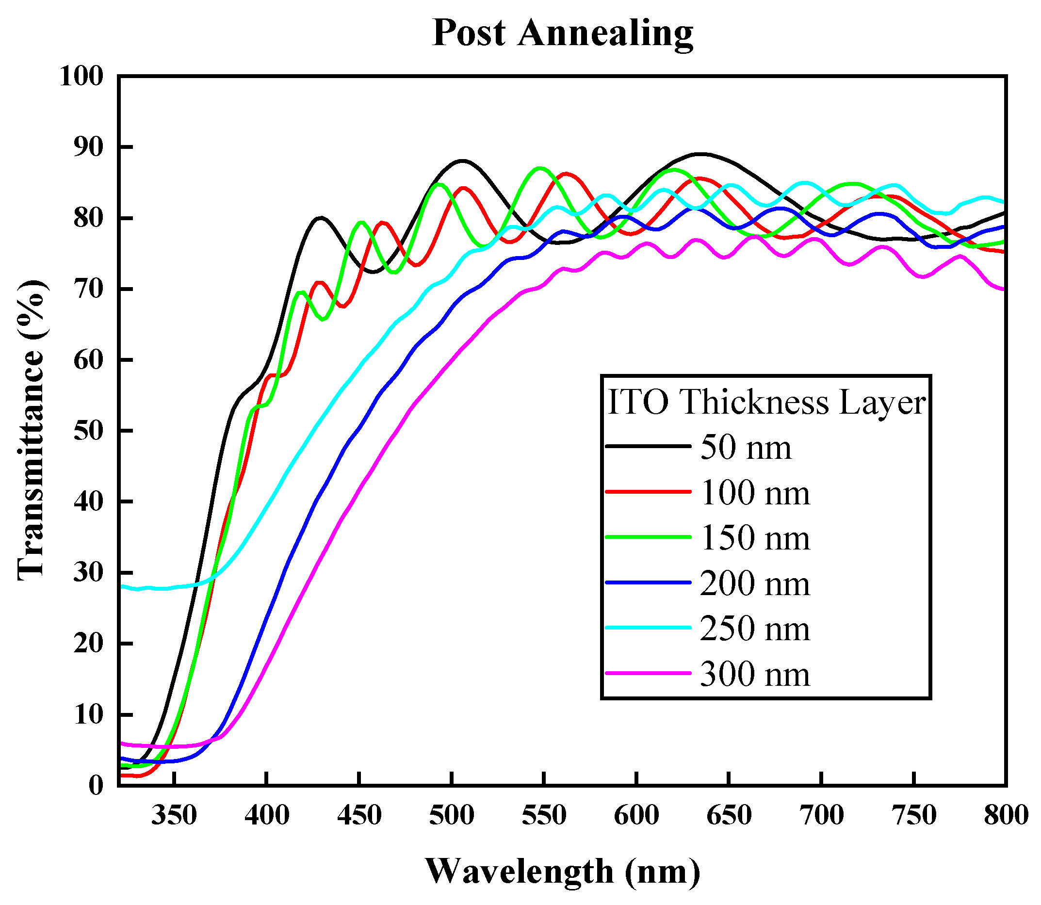
The final and most important property of ITO, which enables it to be installed or built into solar devices as the front electrode, is the transparency of the ITO film grown on the glass substrate. Initially, the silica low-iron glass substrate had a transmittance value of 94%. As can be seen in Figure 7, the transparency values prior to annealing were all below 85% [33,39,40], which are very poor transparency values due to the darker color of the ITO and the reflective properties it had before annealing. Furthermore, the post-annealing transparency (Figure 8) increased significantly in all samples with the best values observed in the films with thicknesses of 50 nm, 100 nm, and 150 nm with transparency values of 89%, 86.16%, and 86.92% at wavelengths of 635 nm, 560 nm, and 550 nm, respectively. This result indicates that these are highly transparent films that can be used for third-generation solar-cell applications [41]. Again, annealing the ITO samples was proven to improve the transmittance due to increasing the charge carrier numbers, with a better crystal quality and a decrease in grain boundary scattering as the grain sizes increased with temperature [42]. Although the 150 nm and 50 nm thicknesses showed better transparency values, they had a lower electrical quality compared to the 100 nm film.
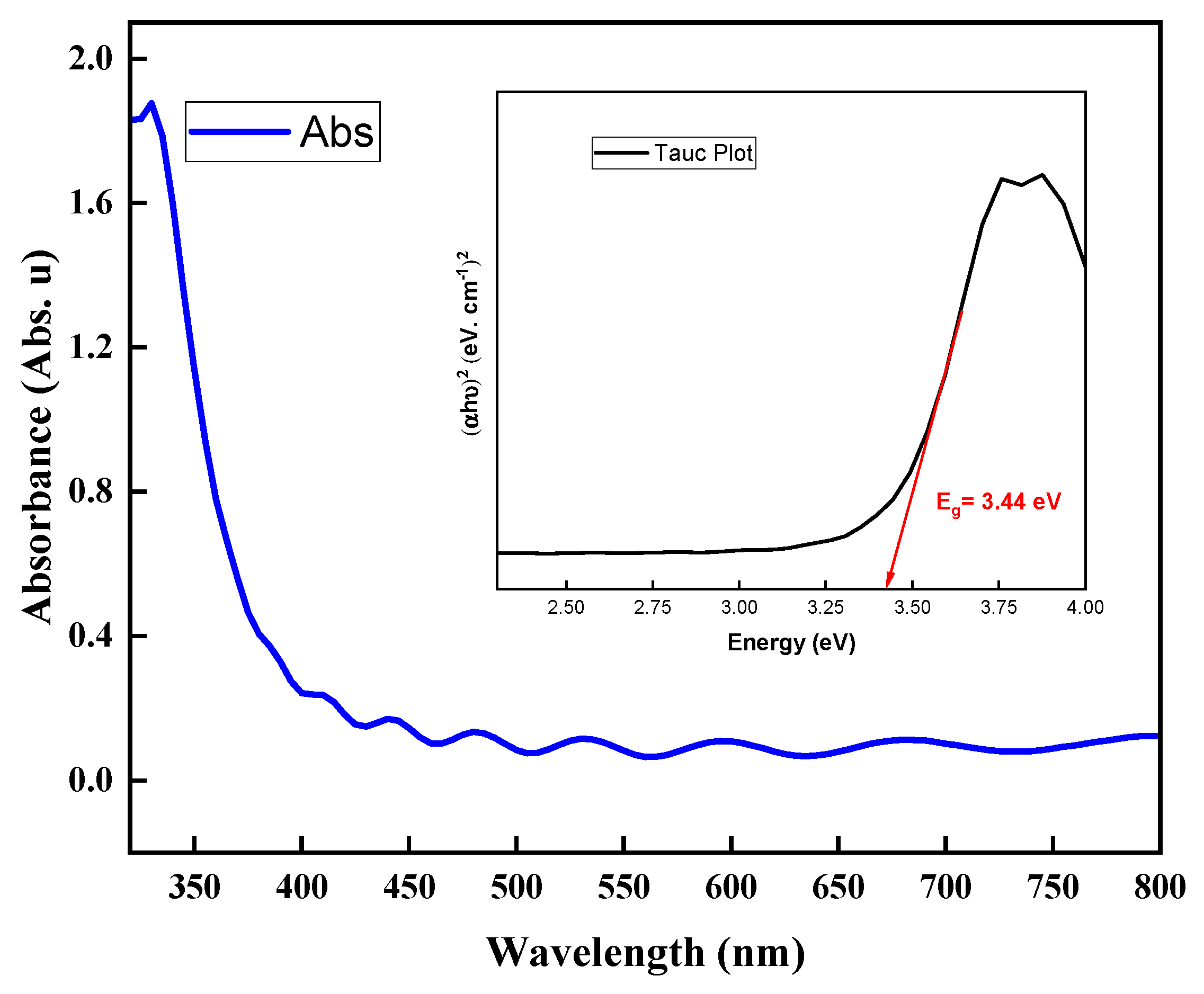
Through our examination of the results, we found that the best thickness was 100 nm in terms of physical, electrical, and optical properties. Thus, we calculated the absorbance (A) of this sample using the transmittance data and Equation (2):
Figure 9 illustrates the resulting absorbance which was in the range of 0.1 to 0.2 Abs.u, indicating a highly favorable range [43,44], as the lowest absorbance possible is desirable for the application of electrodes in third-generation solar cells [7,45,46,47]. We used the absorbance to determine the bandgap using a Tauc plot, as shown in the inset of Figure 9. The resulting bandgap was 3.44 eV [48,49]. We validated the bandgap using the methods used by Jose C.S. Costa et al. [50] and Dariush Souri et al. [51] which indicated that the ITO film had highly transmittance and required the lowest energy from a photon to create voltage in any solar-cell circuit [52,53,54,55].
To provide more insights into our work, Table 1 summarizes the significant results of this study and compares them to those of previous studies.
4. Conclusions
In our recent research conducted at the ESI labs, we explored the growth of indium tin oxide (ITO) thin films using RF magnetron sputtering with argon gas. This approach is relevant for optoelectronic applications, particularly for third-generation solar cells. Through the various film thicknesses tested, we discovered that the films exhibited exceptional physical, electrical, and optical properties. However, the optimal thickness was identified as 100 nm. This particular thickness was distinguished by its remarkable transparency, exceeding 86%; low absorbance, ranging between 0.1 to 0.2 Abs.u; good bandgap energy of 3.44 eV coupled with superior electrical conductivity reaching about 1.86 × 10⁶ S/m; and low resistivity values of approximately 5.3 × 10⁻⁷ Ωm. These characteristics are crucial for ensuring the efficiency of optoelectronic devices used in the field of third-generation solar cells. Our SEM analysis confirmed that the surface morphology of these films was crack-free and validated the thicknesses achieved. Additionally, the ATM assessments indicated a uniform and gradual growth of the thin films with excellent RMS roughness values. Furthermore, the XRD analyses provided insights into the crystalline structure of the films, affirming their suitability for third-generation solar-cell applications. This research underscores the efficiency of RF magnetron sputtering in creating high-quality ITO films, with the 100 nm film particularly demonstrating promising properties for future technological innovations and competing with commercial ITO.
Author Contributions
Methodology, investigation, formal analysis, software, validation, writing—original draft, and resources, H.I.A.; methodology, investigation, formal analysis, validation, and writing—review and editing, F.M.A.; conceptualization, validation, writing—review and editing, and visualization, S.B.; conceptualization, writing—review and editing, supervision, project administration, and funding acquisition, T.M. All authors have read and agreed to the published version of the manuscript.
Funding
The work is partially funded through Engineering and Physical Science Research Council (EP/S030786/1) funded End Use Energy Demand Technology projects to the University of Exeter. For the purpose of open access, the author has applied a Creative Commons Attribution (CC BY) license to any Author Accepted Manuscript version arising from this submission.
Data Availability Statement
The data presented in this study are available upon request from the corresponding author.
Acknowledgments
H. Alabdan and F. Alsahli would like to duly acknowledge the financial support of the Saudi Arabia Culture Bureau in the United Kingdom. The authors thank Dr Hong Chang, Imaging Suite Manager at the Harrison Building, University of Exeter, Streatham Campus, U.K., for their training and technical assistance with the SEM, AFM, and XRD characterizations.
Conflicts of Interest
The authors declare no conflicts of interest and the funders had no role in the design of the study; in the collection, analyses, or interpretation of data; in the writing of the manuscript; or in the decision to publish the results.
References
- Tchenka, A.; Agdad, A.; Samba Vall, M.C.; Hnawi, S.K.; Narjis, A.; Nkhaili, L.; Ibnouelghazi, E.; Ech-Chamikh, E.; Zheludkevich, M. Effect of RF Sputtering Power and Deposition Time on Optical and Electrical Properties of Indium Tin Oxide Thin Film. Adv. Mater. Sci. Eng. 2021, 2021, 5556305. [Google Scholar] [CrossRef]
- Stadler, A. Transparent Conducting Oxides—An Up-to-Date Overview. Materials 2012, 5, 661–683. [Google Scholar] [CrossRef] [PubMed]
- Klaus, E. Magnetron sputtering of transparent conductive zinc oxide: Relation between the sputtering parameters and the electronic properties. J. Phys. D Appl. Phys. 2000, 33, R17. [Google Scholar]
- Klein, A.; Korber, C.; Wachau, A.; Sauberlich, F.; Gassenbauer, Y.; Harvey, S.P.; Proffit, D.E.; Mason, T.O. Transparent Conducting Oxides for Photovoltaics: Manipulation of Fermi Level, Work Function and Energy Band Alignment. Materials 2010, 3, 4892–4914. [Google Scholar] [CrossRef] [PubMed]
- Barman, B.; Swami, S.K.; Dutta, V. Fabrication of highly conducting ZnO/Ag/ZnO and AZO/Ag/AZO transparent conducting oxide layers using RF magnetron sputtering at room temperature. Mater. Sci. Semicond. Process. 2021, 129, 105801. [Google Scholar] [CrossRef]
- Noh, J.H.; Lee, S.; Kim, J.Y.; Lee, J.-K.; Han, H.S.; Cho, C.M.; Cho, I.S.; Jung, H.S.; Hong, K.S. Functional Multilayered Transparent Conducting Oxide Thin Films for Photovoltaic Devices. J. Phys. Chem. C 2009, 113, 1083–1087. [Google Scholar] [CrossRef]
- Hung, C.M.; Mai, C.L.; Wu, C.C.; Chen, B.H.; Lu, C.H.; Chu, C.C.; Wang, M.C.; Yang, S.D.; Chen, H.C.; Yeh, C.Y.; et al. Self-Assembled Monolayers of Bi-Functionalized Porphyrins: A Novel Class of Hole-Layer-Coordinating Perovskites and Indium Tin Oxide in Inverted Solar Cells. Angew. Chem. Int. Ed. Engl. 2023, 62, e202309831. [Google Scholar] [CrossRef]
- Dao, V.A.; Choi, H.; Heo, J.; Park, H.; Yoon, K.; Lee, Y.; Kim, Y.; Lakshminarayan, N.; Yi, J. rf-Magnetron sputtered ITO thin films for improved heterojunction solar cell applications. Curr. Appl. Phys. 2010, 10, S506–S509. [Google Scholar] [CrossRef]
- Sousa, M.G.; da Cunha, A.F. Optimization of low temperature RF-magnetron sputtering of indium tin oxide films for solar cell applications. Appl. Surf. Sci. 2019, 484, 257–264. [Google Scholar] [CrossRef]
- Kurdesau, F.; Khripunov, G.; da Cunha, A.F.; Kaelin, M.; Tiwari, A.N. Comparative study of ITO layers deposited by DC and RF magnetron sputtering at room temperature. J. Non-Cryst. Solids 2006, 352, 1466–1470. [Google Scholar] [CrossRef]
- Amalathas, A.P.; Alkaisi, M.M. Effects of film thickness and sputtering power on properties of ITO thin films deposited by RF magnetron sputtering without oxygen. J. Mater. Sci. Mater. Electron. 2016, 27, 11064–11071. [Google Scholar] [CrossRef]
- Yang, S.; Sun, B.; Liu, Y.; Zhu, J.; Song, J.; Hao, Z.; Zeng, X.; Zhao, X.; Shu, Y.; Chen, J.; et al. Effect of ITO target crystallinity on the properties of sputtering deposited ITO films. Ceram. Int. 2020, 46, 6342–6350. [Google Scholar] [CrossRef]
- Kudryashov, D.; Gudovskikh, A.; Zelentsov, K. Low temperature growth of ITO transparent conductive oxide layers in oxygen-free environment by RF magnetron sputtering. J. Phys. Conf. Ser. 2013, 461, 012021. [Google Scholar] [CrossRef]
- Tchenka, A.; Agdad, A.; Bousseta, M.; El Mouncharih, A.; Amiri, L.; Nkhaili, L.; Narjis, A.; Ibnouelghazi, E.; Ech-Chamikh, E.M. Effect of vacuum annealing and position of metal Cu on structural, optical, electrical and thermoelectrical properties of ITO/Cu/ITO multilayers prepared by RF sputtering. Opt. Mater. 2022, 131, 112634. [Google Scholar] [CrossRef]
- Ahmed, N.M.; Sabah, F.A.; Abdulgafour, H.I.; Alsadig, A.; Sulieman, A.; Alkhoaryef, M. The effect of post annealing temperature on grain size of indium-tin-oxide for optical and electrical properties improvement. Results Phys. 2019, 13, 102159. [Google Scholar] [CrossRef]
- Gupta, L.; Mansingh, A.; Srivastava, P.K. Band gap narrowing and the band structure of tin-doped indium oxide films. Thin Solid Film. 1989, 176, 33–44. [Google Scholar] [CrossRef]
- Jiang, H.; Zhao, Y.; Ma, H.; Wu, Y.; Chen, M.; Wang, M.; Zhang, W.; Peng, Y.; Leng, Y.; Cao, Z.; et al. Broad-Band Ultrafast All-Optical Switching Based on Enhanced Nonlinear Absorption in Corrugated Indium Tin Oxide Films. ACS Nano 2022, 16, 12878–12888. [Google Scholar] [CrossRef] [PubMed]
- Thirumoorthi, M.; Thomas Joseph Prakash, J. Structure, optical and electrical properties of indium tin oxide ultra thin films prepared by jet nebulizer spray pyrolysis technique. J. Asian Ceram. Soc. 2018, 4, 124–132. [Google Scholar] [CrossRef]
- Xu, Y.; Wan, G.; Ma, L.; Zhang, Y.; Su, Y.; Liu, D.; Wang, G. Indium tin oxide as a dual-band compatible stealth material with low infrared emissivity and strong microwave absorption. J. Mater. Chem. C 2023, 11, 1754–1763. [Google Scholar] [CrossRef]
- Kim, J.H.; Jeon, K.A.; Kim, G.H.; Lee, S.Y. Electrical, structural, and optical properties of ITO thin films prepared at room temperature by pulsed laser deposition. Appl. Surf. Sci. 2006, 252, 4834–4837. [Google Scholar] [CrossRef]
- Izumi, H.; Ishihara, T.; Yoshioka, H.; Motoyama, M. Electrical properties of crystalline ITO films prepared at room temperature by pulsed laser deposition on plastic substrates. Thin Solid Film. 2002, 411, 32–35. [Google Scholar] [CrossRef]
- Li, J.; Jiang, L.; Chen, M.; Li, X.; Wei, Y.; Ma, Y.; Fu, Z.; Yan, Y. Structure and physical properties evolution of ITO film during amorphous-crystalline transition using a highly effective annealing technique. Ceram. Int. 2019, 45, 16214–16225. [Google Scholar] [CrossRef]
- Jung, S.K.; Kim, M.C.; Sohn, S.H.; Park, D.K.; Lee, S.H.; Park, L.S. Properties of Indium Tin Oxide on Polymer Films Deposited by Low-Frequency Magnetron Sputtering Method. Mol. Cryst. Liq. Cryst. 2006, 459, 167–177. [Google Scholar] [CrossRef]
- Xu, M.; Hu, S.; Peng, C.; Jing, B.; Chen, L.; Li, X.; Zhang, J. High-Performance Full-Solution-Processed Oxide Thin-Film Transistor Arrays Fabricated by Ultrafast Scanning Diode Laser. Adv. Mater. Interfaces 2022, 9, 2200976. [Google Scholar] [CrossRef]
- Carvalho, R.M.; Santos, L.; Bastos, M.; Costa, J.C.S. Carbon-Induced Changes in the Morphology and Wetting Behavior of Ionic Liquids on the Mesoscale. Langmuir 2024, 40, 3949–3961. [Google Scholar] [CrossRef] [PubMed]
- Tak, Y.-H.; Kim, K.-B.; Park, H.-G.; Lee, K.-H.; Lee, J.-R. Criteria for ITO (indium–tin-oxide) thin film as the bottom electrode of an organic light emitting diode. Thin Solid Film. 2002, 411, 12–16. [Google Scholar] [CrossRef]
- Raoufi, D.; Hosseinpanahi, F. The effect of film thickness on surface morphology of ITO thin films. J. Theor. Appl. Phys. 2013, 7, 21. [Google Scholar] [CrossRef]
- Kavei, G.; Zare, Y.; Mohammadi Gheidari, A. Evaluation of surface roughness and nanostructure of indium tin oxide (ITO) films by atomic force microscopy. Scanning 2008, 30, 232–239. [Google Scholar] [CrossRef] [PubMed]
- Hao, L.; Diao, X.; Xu, H.; Gu, B.; Wang, T. Thickness dependence of structural, electrical and optical properties of indium tin oxide (ITO) films deposited on PET substrates. Appl. Surf. Sci. 2008, 254, 3504–3508. [Google Scholar] [CrossRef]
- Mizuhashi, M. Electrical properties of vacuum-deposited indium oxide and indium tin oxide films. Thin Solid Film. 1980, 70, 91–100. [Google Scholar] [CrossRef]
- Li, H.; Yang, Y.; Liang, X.; Zhang, W.; Cao, L.; Wu, C.; Zeng, Z.; Wang, L. Effect of annealing temperature and time on the microstructure, mechanical properties and conductivity of cold-rolled explosive Cu/Al composite sheets. Mater. Res. Express 2020, 7, 106502. [Google Scholar] [CrossRef]
- Granqvist, C.G.; Hultåker, A. Transparent and conducting ITO films: New developments and applications. Thin Solid Film. 2002, 411, 1–5. [Google Scholar] [CrossRef]
- Chen, Z.; Li, W.; Li, R.; Zhang, Y.; Xu, G.; Cheng, H. Fabrication of highly transparent and conductive indium-tin oxide thin films with a high figure of merit via solution processing. Langmuir 2013, 29, 13836–13842. [Google Scholar] [CrossRef]
- Ederth, J.; Heszler, P.; Hultåker, A.; Niklasson, G.A.; Granqvist, C.G. Indium tin oxide films made from nanoparticles: Models for the optical and electrical properties. Thin Solid Film. 2003, 445, 199–206. [Google Scholar] [CrossRef]
- Haschke, J.; Lemerle, R.; Aissa, B.; Abdallah, A.A.; Kivambe, M.M.; Boccard, M.; Ballif, C. Annealing of Silicon Heterojunction Solar Cells: Interplay of Solar Cell and Indium Tin Oxide Properties. IEEE J. Photovolt. 2019, 9, 1202–1207. [Google Scholar] [CrossRef]
- Gulen, M.; Yildirim, G.; Bal, S.; Varilci, A.; Belenli, I.; Oz, M. Role of annealing temperature on microstructural and electro-optical properties of ITO films produced by sputtering. J. Mater. Sci. Mater. Electron. 2012, 24, 467–474. [Google Scholar] [CrossRef]
- Krasilnikova Sytchkova, A.; Grilli, M.L.; Boycheva, S.; Piegari, A. Optical, electrical, structural and microstructural characteristics of rf sputtered ITO films developed for art protection coatings. Appl. Phys. A 2007, 89, 63–72. [Google Scholar] [CrossRef]
- Ghorannevis, Z.; Akbarnejad, E.; Ghoranneviss, M. Structural and morphological properties of ITO thin films grown by magnetron sputtering. J. Theor. Appl. Phys. 2015, 9, 285–290. [Google Scholar] [CrossRef]
- Senthilkumar, V.; Vickraman, P.; Jayachandran, M.; Sanjeeviraja, C. Structural and optical properties of indium tin oxide (ITO) thin films with different compositions prepared by electron beam evaporation. Vacuum 2010, 84, 864–869. [Google Scholar] [CrossRef]
- Salehi, A. The effects of deposition rate and substrate temperature of ITO thin films on electrical and optical properties. Thin Solid Film. 1998, 324, 214–218. [Google Scholar] [CrossRef]
- Farhan, M.S.; Zalnezhad, E.; Bushroa, A.R.; Sarhan, A.A.D. Electrical and optical properties of indium-tin oxide (ITO) films by ion-assisted deposition (IAD) at room temperature. Int. J. Precis. Eng. Manuf. 2013, 14, 1465–1469. [Google Scholar] [CrossRef]
- Ahmed, M.; Bakry, A.; Qasem, A.; Dalir, H. The main role of thermal annealing in controlling the structural and optical properties of ITO thin film layer. Opt. Mater. 2021, 113, 110866. [Google Scholar] [CrossRef]
- van Dam, D.; van Hoof, N.J.; Cui, Y.; van Veldhoven, P.J.; Bakkers, E.P.; Gomez Rivas, J.; Haverkort, J.E. High-Efficiency Nanowire Solar Cells with Omnidirectionally Enhanced Absorption Due to Self-Aligned Indium-Tin-Oxide Mie Scatterers. ACS Nano 2016, 10, 11414–11419. [Google Scholar] [CrossRef] [PubMed]
- Furube, A.; Yoshinaga, T.; Kanehara, M.; Eguchi, M.; Teranishi, T. Electric-field enhancement inducing near-infrared two-photon absorption in an indium-tin oxide nanoparticle film. Angew. Chem. Int. Ed. Engl. 2012, 51, 2640–2642. [Google Scholar] [CrossRef] [PubMed]
- Azani, M.R.; Hassanpour, A.; Torres, T. Benefits, Problems, and Solutions of Silver Nanowire Transparent Conductive Electrodes in Indium Tin Oxide (ITO)-Free Flexible Solar Cells. Adv. Energy Mater. 2020, 10, 2002536. [Google Scholar] [CrossRef]
- Buchholz, D.B.; Proffit, D.E.; Wisser, M.D.; Mason, T.O.; Chang, R.P.H. Electrical and band-gap properties of amorphous zinc–indium–tin oxide thin films. Prog. Nat. Sci. Mater. Int. 2012, 22, 1–6. [Google Scholar] [CrossRef]
- Franzen, S. Surface Plasmon Polaritons and Screened Plasma Absorption in Indium Tin Oxide Compared to Silver and Gold. J. Phys. Chem. C 2008, 112, 6027–6032. [Google Scholar] [CrossRef]
- Dolgonos, A.; Mason, T.O.; Poeppelmeier, K.R. Direct optical band gap measurement in polycrystalline semiconductors: A critical look at the Tauc method. J. Solid State Chem. 2016, 240, 43–48. [Google Scholar] [CrossRef]
- Senol, S.D.; Senol, A.; Ozturk, O.; Erdem, M. Effect of annealing time on the structural, optical and electrical characteristics of DC sputtered ITO thin films. J. Mater. Sci. Mater. Electron. 2014, 25, 4992–4999. [Google Scholar] [CrossRef]
- Costa, J.C.S.; Taveira, R.J.S.; Lima, C.F.R.A.C.; Mendes, A.; Santos, L.M. Optical band gaps of organic semiconductor materials. Opt. Mater. 2016, 58, 51–60. [Google Scholar] [CrossRef]
- Souri, D.; Tahan, Z.E. A new method for the determination of optical band gap and the nature of optical transitions in semiconductors. Appl. Phys. B 2015, 119, 273–279. [Google Scholar] [CrossRef]
- Weijtens, C.H.L.; Van Loon, P.A.C. Influence of annealing on the optical properties of indium tin oxide. Thin Solid Film. 1991, 196, 1–10. [Google Scholar] [CrossRef]
- Kerkache, L.; Layadi, A.; Dogheche, E.; Rémiens, D. Physical properties of RF sputtered ITO thin films and annealing effect. J. Phys. D Appl. Phys. 2006, 39, 184–189. [Google Scholar] [CrossRef]
- Moriga, T.; Okamoto, T.; Hiruta, K.; Fujiwara, A.; Nakabayashi, I.; Tominaga, K. Structures and Physical Properties of Films Deposited by Simultaneous DC Sputtering of ZnO and In2O3 or ITO Targets. J. Solid State Chem. 2000, 155, 312–319. [Google Scholar] [CrossRef]
- Fallah, H.R.; Ghasemi, M.; Hassanzadeh, A.; Steki, H. The effect of annealing on structural, electrical and optical properties of nanostructured ITO films prepared by e-beam evaporation. Mater. Res. Bull. 2007, 42, 487–496. [Google Scholar] [CrossRef]
Figure 1.
The fabrication process of ITO samples.

Figure 2.
X-ray diffraction patterns of ITO films with different thicknesses before annealing.

Figure 3.
X-ray diffraction patterns of ITO films with different thicknesses after annealing.

Figure 4.
AFM images of ITO films with different thicknesses and their respective RMS R values.

Figure 5.
(a) Conductivity (S/m), (b) resistivity (Ωm), and (c) sheet resistance (Ω sq−1) vs. film thickness (nm).
Figure 5.
(a) Conductivity (S/m), (b) resistivity (Ωm), and (c) sheet resistance (Ω sq−1) vs. film thickness (nm).

Figure 6.
SEM images of top and cross-section of ITO films with thicknesses of 50, 100, and 150 nm after annealing.
Figure 6.
SEM images of top and cross-section of ITO films with thicknesses of 50, 100, and 150 nm after annealing.

Figure 7.
Transmittance (%) of films prior to annealing vs. wavelength (nm).

Figure 8.
Transmittance (%) of films after annealing vs. wavelength (nm).

Figure 9.
The absorbance of 100 nm ITO thin film with the calculated bandgap in the inset.


Table 1.
A comprehensive comparison between this work and previous studies.
| Ref. | Year | Gas Type | Thickness (nm) | Annealing Temp (°C) | Electrical Properties | Transparency (%) | Band Gap (eV) | Morphological Properties |
|---|---|---|---|---|---|---|---|---|
| F. Kurdesau et al. [10] | 2006 | Argon–Oxygen | 300–500 | - | - | 80–85 | - | SEM: small-grained (10–20 nm) structure |
| Vinh Ai Dao et al. [8] | 2010 | Argon | 100 ± 5 | 100 | - | 87–90 | 3.67–3.83 | - |
| D Kudryashov et al. [13] | 2013 | Argon | ~100 | - | Resistivity: 5.4 × 10⁻⁴ Ω·cm | 80–90 | - | Smooth surface |
| A. P. Amalathas et al. [11] | 2016 | Argon | 75–225 | - | Average resistivity: 9.4 × 10⁻⁴ Ω·cm | Over 75 | 3.831–4.003 | AFM: surface roughness increased with thickness |
| Shumin Yang et al. [12] | 2020 | Oxygen | ~150 | 300 | - | 89.02–90.7 | 3.60–3.67 | - |
| This work | 2024 | Argon | 100 | 500 | Resistivity range: 1–2 × 10⁻⁴ Ω·cm | 86.16–89.0 | 3.44 | Low RMS roughness values |
Disclaimer/Publisher’s Note: The statements, opinions and data contained in all publications are solely those of the individual author(s) and contributor(s) and not of MDPI and/or the editor(s). MDPI and/or the editor(s) disclaim responsibility for any injury to people or property resulting from any ideas, methods, instructions or products referred to in the content. |
© 2024 by the authors. Licensee MDPI, Basel, Switzerland. This article is an open access article distributed under the terms and conditions of the Creative Commons Attribution (CC BY) license (https://creativecommons.org/licenses/by/4.0/).
Share and Cite
MDPI and ACS Style
Alabdan, H.I.; Alsahli, F.M.; Bhandari, S.; Mallick, T. Monolithic Use of Inert Gas for Highly Transparent and Conductive Indium Tin Oxide Thin Films. Nanomaterials 2024, 14, 565. https://doi.org/10.3390/nano14070565
AMA Style
Alabdan HI, Alsahli FM, Bhandari S, Mallick T. Monolithic Use of Inert Gas for Highly Transparent and Conductive Indium Tin Oxide Thin Films. Nanomaterials. 2024; 14(7):565. https://doi.org/10.3390/nano14070565
Chicago/Turabian StyleAlabdan, Hessa I., Fahad M. Alsahli, Shubhranshu Bhandari, and Tapas Mallick. 2024. "Monolithic Use of Inert Gas for Highly Transparent and Conductive Indium Tin Oxide Thin Films" Nanomaterials 14, no. 7: 565. https://doi.org/10.3390/nano14070565
Note that from the first issue of 2016, this journal uses article numbers instead of page numbers. See further details here.